– 33 –
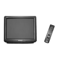
KV-HS29M61/M90/M91, HS34M61/M90/M91, HS38M61/M90/M91
RM-997
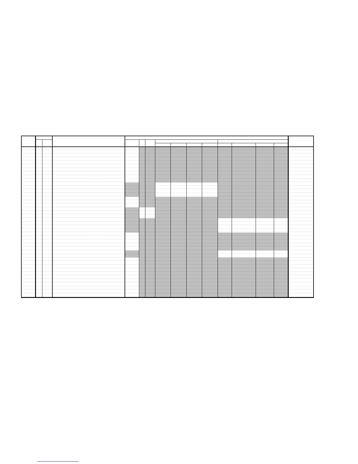
Category Item Function Standard Data Device Name
No. Name Common TV Video 3D-Comb NR Mode Picture/Sound Mode Table (Slave Address)
NRmode0 NRmode1 NRmode2 NRmode3 Dynamic Standard/Drama Hi-Fine/Soft Personal
3CM 00 NRM Noise Reduction Operation Mode 00 UPD64083 (B8H)
01 YCO Y/C Signal Output Selection 0D
02 SYC System Clock Selection 01
03 STD Standard/Non-standard Operation Selection 00
04 MSS Inter-frame/Inter-line Operation Selection 00
05 KIL Killer/Non-killer Operation Selection 00
06 ECS External C-sync Input Selection 01
07 CPP ADC Input Level & Clump Pulse Width Selection 00
08 HDP Horizontal Phase Adjustment 05
09 CDL C-signal delay Adjustment 04
0A DYC DY Detection Coring Level Adjustment 02 02 02 04
0B DYG DY Detection Gain Adjustment 0A 0A 0A 0A
0C DCC DC Detection Coring Level Adjustment 05 03 03 05
0D DCG DC Detection Gain Adjustment 05 0A 0A 05
0E YNR YNR Non-linear Filter Setup 01
0F CNR CNR Non-linear Filter Setup 01
10 WSC Noise Detectin Coring Adjustment 01
11 VTH Hysteresis Selection for H-sync Non-standard 01 01
12 VTR Sensitivity Selection for H-sync Non-standard 01 01
13 LDR Sensitivity Selection for Frame-sync Non-standard 02 01
14 VAP Gain Adjustment for Vertical Shape Correction 00 00 00 00
15 VAI Vanishing Adjustment for Vertical Shape Correction 00 00 00 00
16 YPF Center Frequency Selection for Y-peaking BPF 03 03 03 03
17 YPG Gain Adjustment for Y-peaking BPF 0A 08 08 08
18 VSE Line Comb Filter Setup 02
19 CCN C-signal Split Filter Switch 00
1A COS C-signal Delay Switch at Noise Reduction 00
1B SDC DC Detection Sensitivity Switch 00
1C SDY DY Detection Lower-level Sensitivity Switch 01
1D YHC Y-signal Higher-level Coring Selection 00 00 00 00
1E YHG Y-signal Higher-level Gain Switch 00 00 00 00
1F SHT Non-standard Detection & H/V Counter Test Bits 00
20 CLK Clock Test Bits 08
21 PLL PLL Filter Setup 0D
22 KRF Killer Detection Reference Adjustment 03
23 HSL H-sync Slice Level Adjustment 0C
24 VSL V-sync Slice Level Adjustment 08
25 BPS Internal Burst Gate Start Position Adjustment 04
26 BPW Internal Burst Gate Width Adjustment 0A
27 ADC ADC Clock Delay Selection 03
28 APD ADC Power-down Switch 01
29 SPD Memory Power-down Switch 00
 Loading...