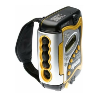
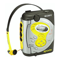
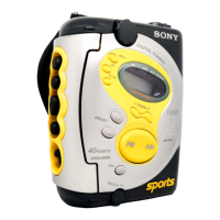
WM-FS421
1212
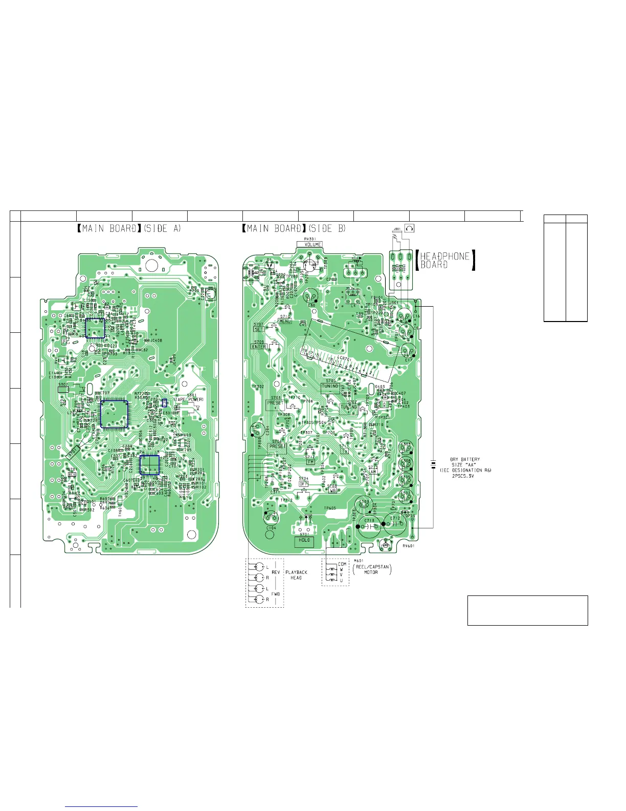
6-3. PRINTED WIRING BOARD
Note on Printed Wiring Board:
• X : parts extracted from the component side.
• Y : parts extracted from the conductor side.
• b : Pattern from the side which enables seeing.
Ref. No. Location
D1 A-5
D2 B-2
D4 B-2
D403 D-7
D404 D-7
D701 F-7
IC1 B-2
IC301 E-3
IC701 D-3
IC702 D-2
Q3 C-3
Q200 A-5
Q301 E-3
Q501 F-2
Q502 E-1
Q701 E-1
• Semiconductor
Location
w
Y
>
HP701
0FF - ON
L3
AM
FERRIRE.ROD
ANTENNA
TP2
TP1
TP(VCO)
12
A
B
C
D
E
F
G
3456789
IC702
IC301
IC701
IC1
Caution:
Pattern face side: Parts on the pattern face side seen from
(Side A) the parts face are indicated.
Parts face side: Parts on the parts face side seen from
(Side B) the pattern face are indicated.
 Loading...