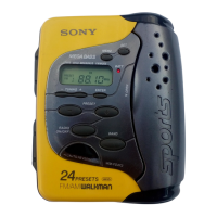
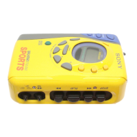
WM-FS421
1313
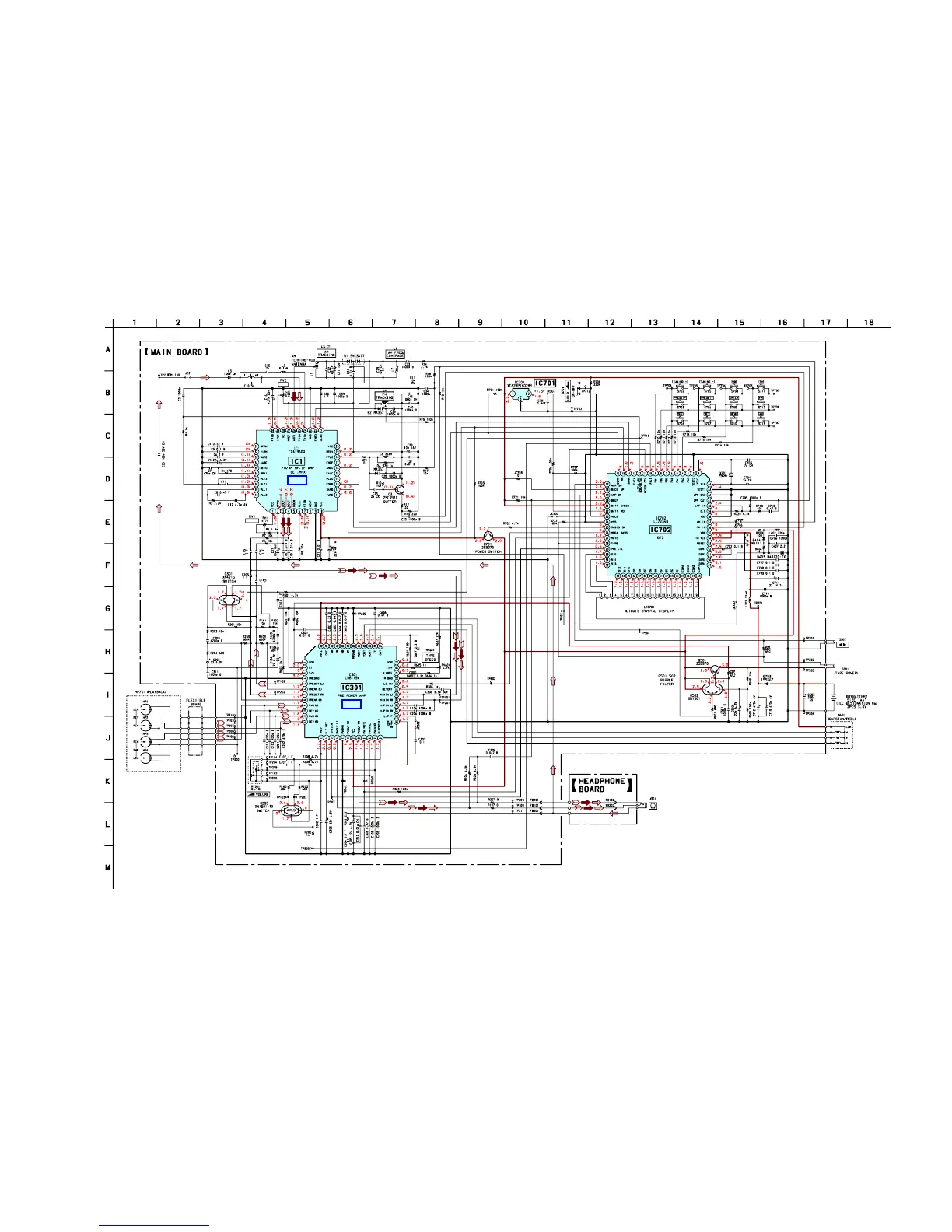
6-4. SCHEMATIC DIAGRAM
Note on Schematic Diagram:
• All capacitors are in µF unless otherwise noted. pF: µµF
50 WV or less are not indicated except for electrolytics
and tantalums.
• All resistors are in Ω and
1
/
4
W or less unless other-
wise specified.
• C : panel designation.
• A : B+ Line.
• H : adjustment for repair.
• Power voltage is dc 3 V and fed with regulated dc power
supply from battery terminal.
• Voltages are dc with respect to ground under no-signal
(detuned) conditions.
no mark : PB
( ) : FM
• Voltages are taken with a VOM (Input impedance 10 MΩ).
Voltage variations may be noted due to normal produc-
tion tolerances.
• Signal path.
F : FM
f : AM
E : PB
• Refer to page 10 for IC Block Diagrams.
• Refer to page 17 for IC Pin Function.
IC B/D
IC B/D
AM IF
FM VCO

 Loading...