OPERATION
2-5
been programmed with the vernier setting, none of the primary drive voltage LEDs will be on. To return to the
primary output levels, press the [Select] key. The output voltage will be increased to the next highest primary
level.
The output voltage is applied to the device under test through a source
impedance, thus, the voltage across the device is always less than or equal to the
output voltage. The different source impedances are 25 Ω (R3), 400 Ω (R2),
6.4 kΩ (R1), and 100 kΩ (R0), all accurate to 2 %. The source impedance is
selected as a function of the measurement range, unless the unit is in constant
voltage mode. In the constant voltage mode, the source impedance is always
25 Ω. See the next section for determining which measurement range the unit is
using.
10
8
10
7
10
6
10
5
10
4
10
3
10
2
10
1
10
0
10
-1
0.0
0.2
0.4
0.6
0.8
1.0
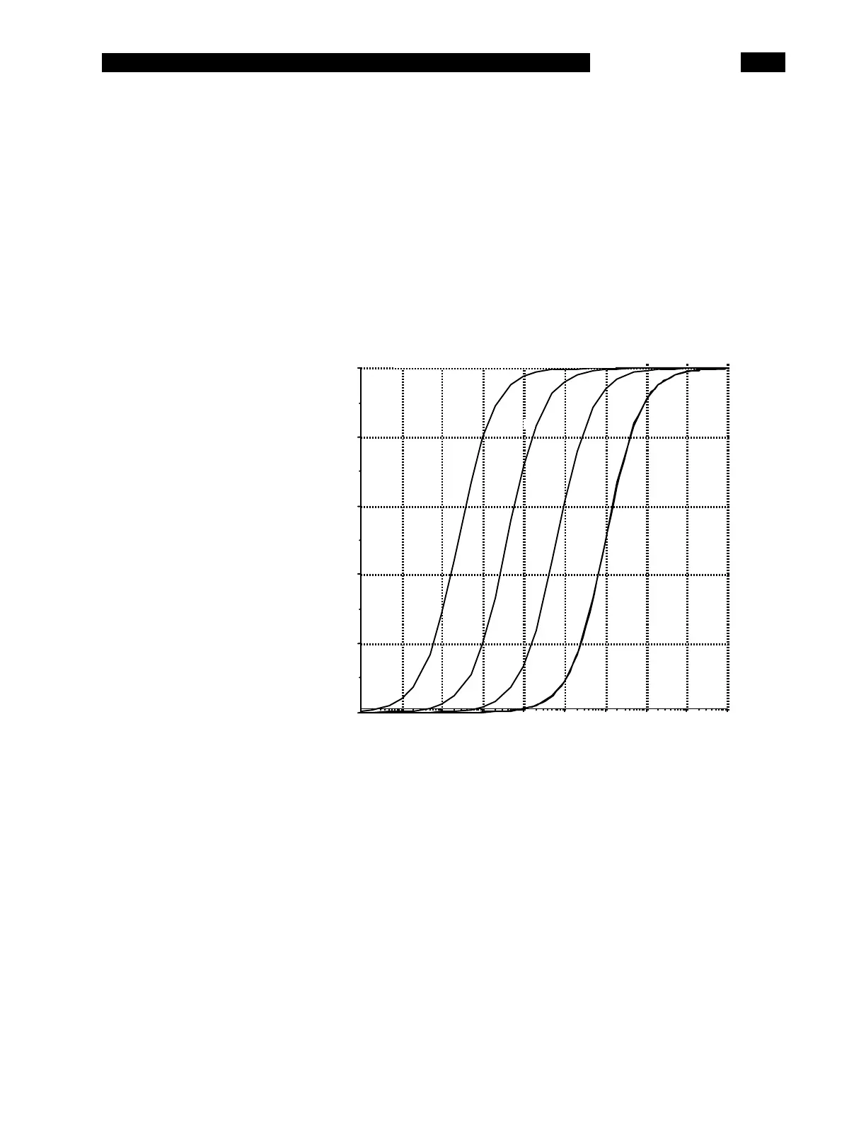
Voltage Across DUT vs DUT Impedance
For Different Ranges
Normalized to 1.0 Volt
DUT Impedance
Volts
R3 or
CV
R2
R1 R0
The graph above shows the voltage across the Device Under Test (DUT) vs the
DUT impedance for the different measurement ranges. The values are
normalized to a 1.0 V output drive setting; for different applied voltages simply
scale the graph values by the applied voltage. Note that the voltage applied to the
DUT is nearly equal to the output voltage at the upper end of each range and
decreases with lower impedance toward the lower end of the range. This is
because of the output source impedance. If the unit is in constant voltage (CV)
mode, the source impedance is always set to 25 Ω. For any impedance
significantly larger than 25 Ω, the voltage across the part is essentially equal to
the output drive voltage.
For most devices, including resistors, most capacitors and many inductors, the
1.0 Vrms setting is the most appropriate setting. For some inductors and active
devices, such as diodes and transistors, the 0.25 or 0.10 Vrms setting should be
used. Certain devices require a specific test voltage, such as Z5U ceramic disk
 Loading...