Hardware configuration UM1075
14/20 UM1075 Rev 10
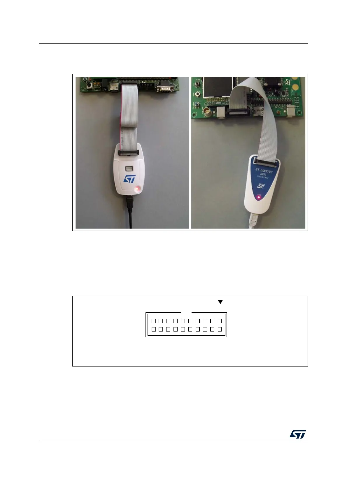
Figure 9 shows how to connect the ST-LINK/V2 to a target using the JTAG cable.
Figure 9. JTAG and SWD connection
1. A = Target application board with JTAG connector
2. B = JTAG/SWD 20-wire flat cable
3. C = STM32 JTAG and SWD target connector
The reference of the connector needed on the target application board is:
2x10C header wrapping 2x40C H3/9.5 (pitch 2.54) - HED20 SCOTT PHSD80.
Figure 10. JTAG debugging flat ribbon layout
Note: For low-cost applications, or when the standard 20-pin 2.54 mm-pitch connector footprint is
too large, it is possible to implement the TAG-Connect solution. The TAG-Connect adapter
and cable provide a simple and reliable means of connecting ST-LINK/V2 or ST-LINK/V2-
ISOL to the PCB without requiring a mating component on the application PCB.
Viewed from above PCB
19 17 15 13 11 9 7 5 3 1
20 18 16 14 12 10 8 6 4 2
ai18744