Contents
1 Features...........................................................................2
2 Ordering information ..............................................................3
2.1 Codification ...................................................................3
3 Development environment .........................................................4
3.1 System requirements ...........................................................4
3.2 Development toolchains .........................................................4
3.3 Demonstration software .........................................................4
4 Conventions.......................................................................5
5 Quick start ........................................................................6
5.1 Getting started .................................................................6
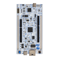
6 Hardware layout and configuration.................................................7
6.1 STM32 Nucleo-64 board mechanical drawing......................................10
6.2 Default board configuration .....................................................11
6.3 Cuttable PCB.................................................................11
6.4 Embedded ST-LINK/V2-1.......................................................11
6.4.1 Drivers ...............................................................11
6.4.2 ST-LINK/V2-1 firmware upgrade ............................................12
6.4.3 Using ST-LINK/V2-1 to program/debug the on-board STM32 ......................12
6.4.4 Using ST-LINK/V2-1 to program/debug an external STM32 application ..............12
6.5 Power supply and power selection ...............................................13
6.5.1 External power supply input ...............................................13
6.5.2 External power supply output ..............................................14
6.6 Programming/debugging when the power supply is not from ST-LINK .................14
6.7 OSC clock sources ............................................................14
6.7.1 LSE clock reference .....................................................15
6.7.2 HSE clock reference .....................................................15
6.8 Reset sources ................................................................15
6.9 VCP communication ...........................................................16
6.10 LEDs........................................................................16
6.11 Push‑buttons .................................................................16
6.12 I
DD
measurement .............................................................16
6.13 Jumper configuration ..........................................................17
6.14 Solder bridge configuration .....................................................17
7 Connectors.......................................................................19
UM2953
Contents
UM2953 - Rev 1
page 28/32