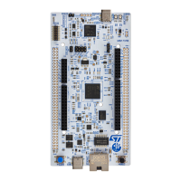
6.13 Jumper configuration
The default jumper positions are shown in Table 4. Table 9 describes the other available jumper settings
Table 9. Jumper configuration
Jumper Definition
State
(1)
Comment
CN2
T_SWCLK
T_SWDIO
[1-2]
[3-4]
ST-LINK/V2-1 enable for
on‑board MCU debugger
OFF
OFF
ST-LINK/V2-1 enable for
external MCU debugger
JP2/JP3 GND ON GND probe
JP5 5 V power selection
[1-2] 5V from ST-LINK
[3-4] 5 V from VIN 7 to 12 V
[5-6] 5 V from E5V
[7-8] 5 V from USB_CHG
OFF No 5 V power
JP1 STLK reset
OFF No STLK reset
[1-2] STLK reset
JP6 IDD measurement
[1-2] VDD = 3.3 V
OFF
To connect the external
source
(ULPBench probe as an
example)
1. Default jumper state is shown in bold.
6.14
Solder bridge configuration
Table 10 describes the solder bridge settings.
Table 10. Solder bridge configuration and settings
Solder bridge Definition
State
(1)
Comment
SB11/SB13/SB15/SB17
SWD interface
(Default)
ON Reserved, do not modify.
SB12/SB14/SB16/SB18
SWD interface
(Reserved)
OFF Reserved, do not modify.
SB21/SB22
VCP interface
(Default)
ON
VCP connects ST-LINK and
on‑board MCU.
VCP interface
(Reserved)
OFF VCP interface used as GPIOs
SB1
Allowed current through CN1
setting
ON
100 mA maximum allowed
current through CN1
OFF
300 mA maximum allowed
current through CN1
SB20 MCO
ON
MCO from STLK provides
8 MHz CLK to MCU.
OFF MCO from STLK floating
UM2953
Jumper configuration
UM2953 - Rev 1
page 17/32