DocID15687 Rev 5 15/29
PM0059 Flash memory interface
28
2.6.2 Programming user option bytes
To run any operation on this sector, the option lock bit (OPTLOCK) in the Flash option
control register (FLASH_OPTCR) must be cleared. To be allowed to clear this bit, you have
to perform the following sequence:
1. Write OPTKEY1 = 0x0819 2A3B in the Flash option key register (FLASH_OPTKEYR)
2. Write OPTKEY2 = 0x4C5D 6E7F in the Flash option key register (FLASH_OPTKEYR)
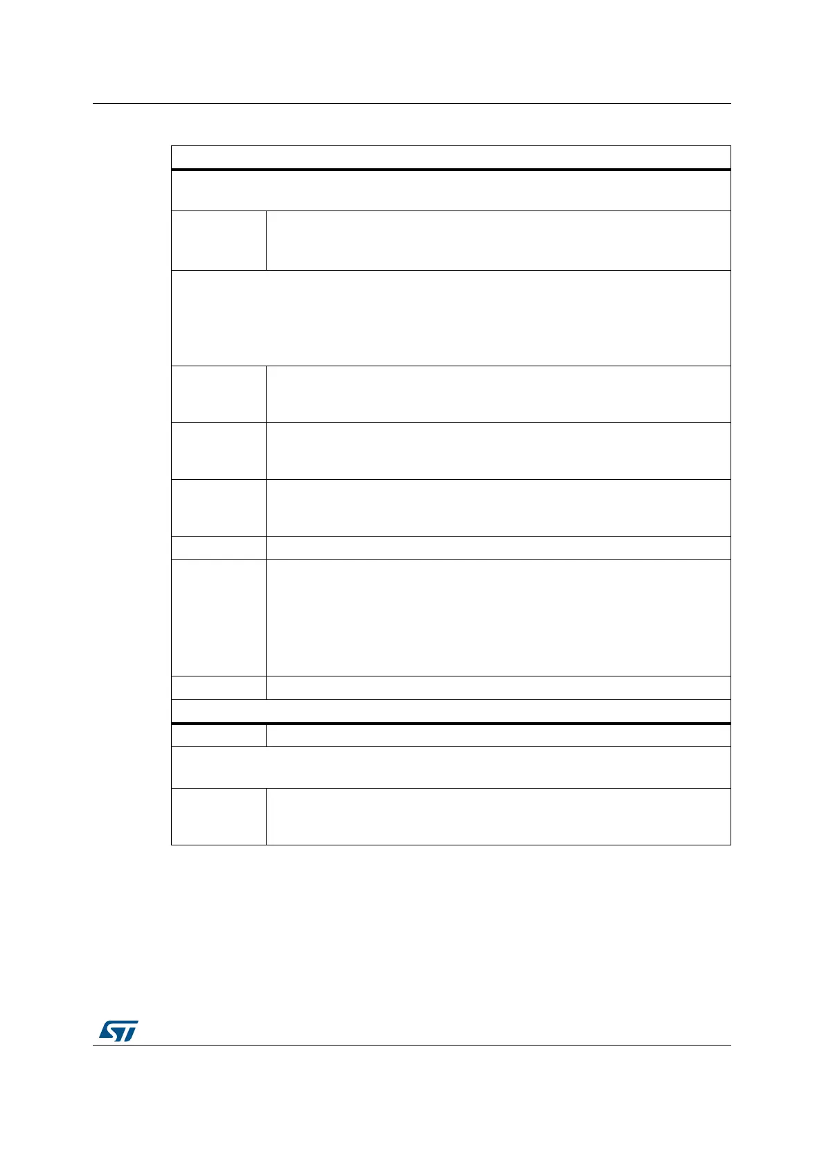
Table 7. Description of the option bytes
Option bytes (word, address 0x1FFF C000)
RDP: Read protection option byte.
The read protection is used to protect the software code stored in Flash memory.
Bits 15:8
0xAA: Level 0, no protection
0xCC: Level 2, chip protection (debug and boot from RAM features disabled)
Others: Level 1, read protection of memories (debug features limited)
USER: User option byte
This byte is used to configure the following features:
– Select the watchdog event: Hardware or software
– Reset event when entering the Stop mode
– Reset event when entering the Standby mode
Bit 7
nRST_STDBY
0: Reset generated when entering the Standby mode
1: No reset generated
Bit 6
nRST_STOP
0: Reset generated when entering the Stop mode
1: No reset generated
Bit 5
WDG_SW
0: Hardware watchdog
1: Software watchdog
Bit 4 0x1: Not used
Bits 3:2
BOR_LEV: BOR reset Level
These bits contain the supply level threshold that activates/releases the reset.
They can be written to program a new BOR level value into Flash memory.
00: BOR Level 3 (VBOR3). reset threshold level from 2.70 to 3.60 V
01: BOR Level 2 (VBOR2). reset threshold level from 2.40 to 2.70 V
10: BOR Level 1 (VBOR1). reset threshold level from 2.10 to 2.40 V
11: BOR off (VBOR0), reset threshold level from 1.8 to 2.10 V
Bits 1:0 0x1: Not used
Option bytes (word, address 0x1FFF C008)
Bits 15:12 0xF: Not used
nWRP: Flash memory write protection option bytes
Sectors 0 to 11 can be write protected.
Bit i
(0 ≤ i ≤ 11)
nWRPi
0: Write protection active on sector i
1: Write protection not active on sector i
 Loading...


