Flash memory interface PM0059
18/29 DocID15687 Rev 5
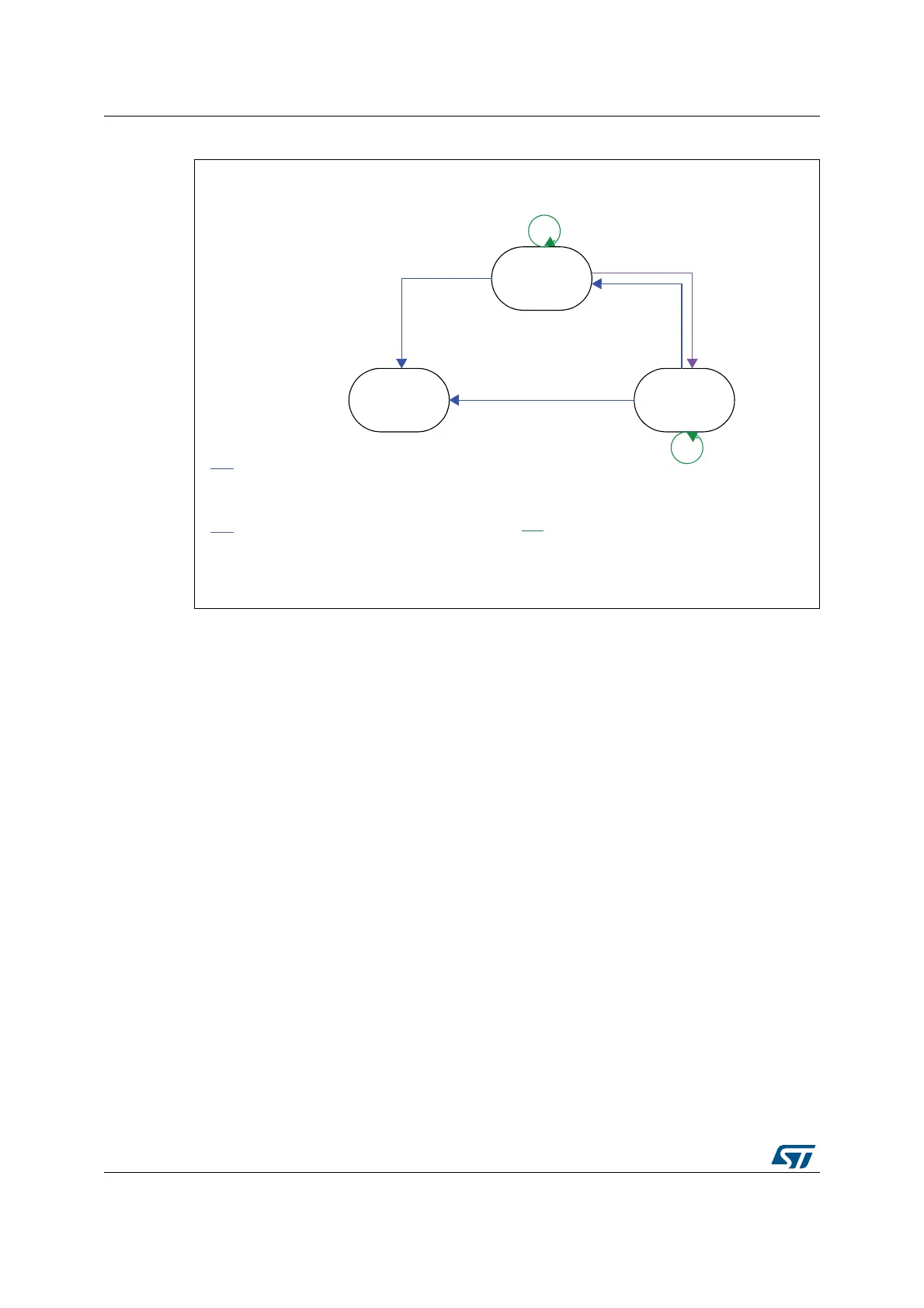
Figure 3. RDP levels
2.6.4 Write protections
The user sectors (0 to 11) in Flash memory can be protected against unwanted write
operations due to loss of program counter contexts. When the not write protection bit in
sector i (nWRPi, 0 ≤ i ≤ 11) is low, the corresponding sector cannot be erased or
programmed. Consequently, a mass erase cannot be performed if one of the sectors is
write-protected.
If an erase/program operation to a write-protected part of the Flash memory is attempted
(sector protected by write protection bit, OTP part locked or part of the Flash memory that
can never be written like the ICP), the write protection error flag (WRPERR) is set in the
FLASH_SR register.
Note: When the memory read protection level is selected (RDP level = 1), it is not possible to
program or erase Flash memory sector i if the CPU debug features are connected (JTAG or
single wire) or boot code is being executed from RAM, even if nWRPi = 1.
,EVEL
LEVE,LEVE,
H!!0$2H##0$2
2$0!!H
2$0##H
DEFAULT
/PTIONSWRITE2$0LEVELINCREASEINCLUDES
/PTIONSERASE
.EWOPTIONSPROGRAM
/PTIONSWRITE2$0LEVELDECREASEINCLUDES
-ASSERASE
/PTIONSERASE
.EWOPTIONSPROGRAM
/PTIONSWRITE2$0LEVELIDENTICALINCLUDES
/PTIONSERASE
.EWOPTIONSPROGRAM
2$0!!H
/THERSOPTIONSMODIFIED
2$0!!H##H
/THERSOPTIONSMODIFIED
7RITEOPTIONS
INCLUDING
2$0!!H
7RITEOPTIONS
INCLUDING
2$0##H
7RITEOPTIONS
INCLUDING
2$0##H
7RITEOPTIONSINCLUDING
2$0##H!!H
AI
 Loading...


