Flash memory interface PM0059
24/29 DocID15687 Rev 5
2.8.6 Flash option control register (FLASH_OPTCR)
The FLASH_OPTCR register is used to modify the user option bytes.
Address offset: 0x14
Reset value: 0x0FFF AAED. The option bits are loaded with values from Flash memory at
reset release.
Access: no wait state when no Flash memory operation is ongoing, word, half-word and
byte access.
Bits 9:8 PSIZE: Program size
These bits select the program parallelism.
00 program x8
01 program x16
10 program x32
11 program x64
Bit 7 Reserved, must be kept cleared.
Bits 6:3 SNB: Sector number
These bits select the sector to erase.
0000 sector 0
0001 sector 1
...
1011 sector 11
Others not allowed
Bit 2 MER: Mass Erase
Erase activated for all user sectors.
Bit 1 SER: Sector Erase
Sector Erase activated.
Bit 0 PG: Programming
Flash programming activated.
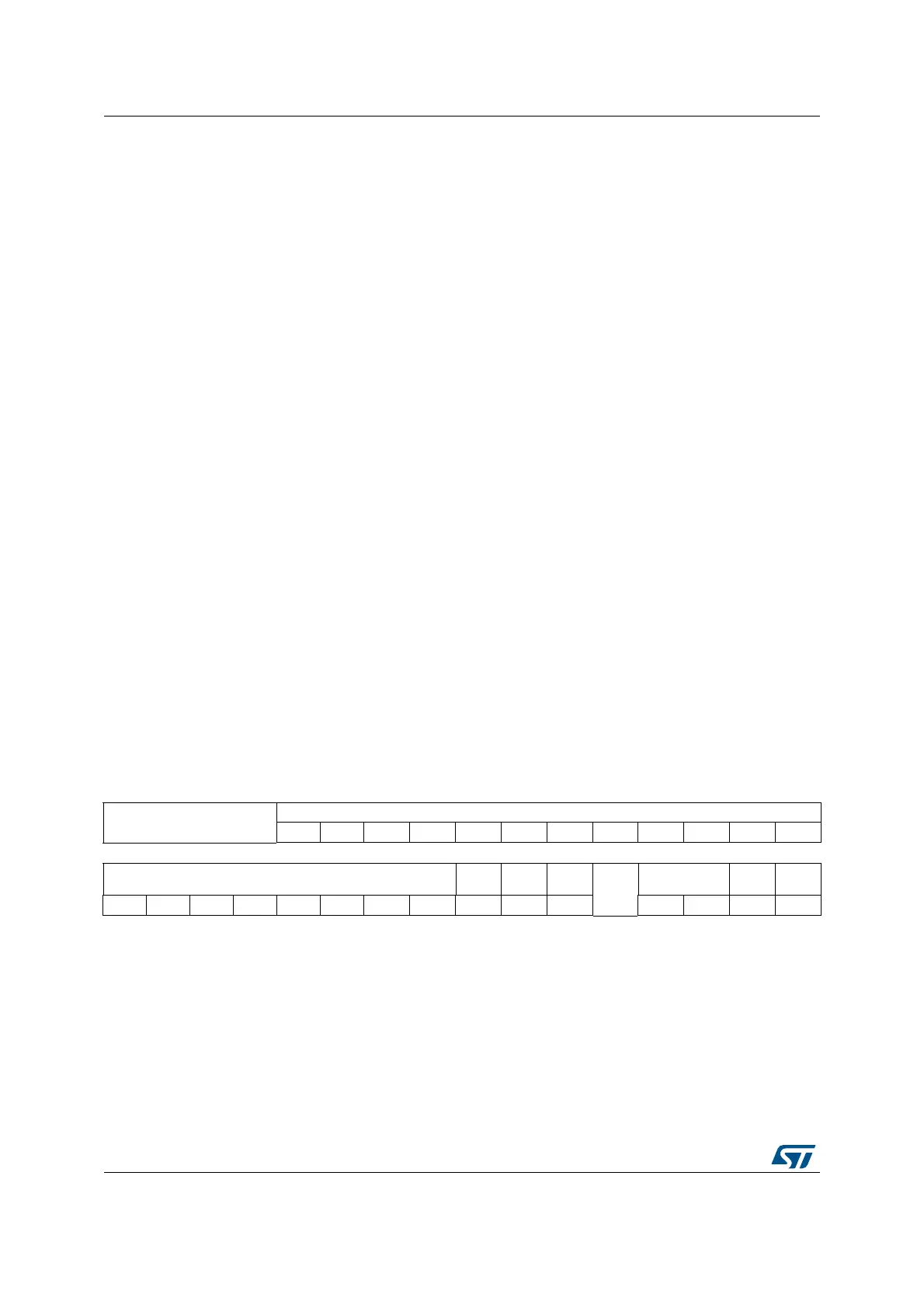
31 30 29 28 27 26 25 24 23 22 21 20 19 18 17 16
Reserved
nWRP[11:0]
rw rw rw rw rw rw rw rw rw rw rw rw
1514131211109876543210
RDP[7:0]
nRST_
STDBY
nRST_
STOP
WDG_
SW
Reserv
ed
BOR_LEV
OPTST
RT
OPTLO
CK
rw rw rw rw rw rw rw rw rw rw rw rw rw rs rs
 Loading...


