Flash memory interface PM0059
20/29 DocID15687 Rev 5
2.8 Flash interface registers
2.8.1 Flash access control register (FLASH_ACR)
The Flash access control register is used to enable/disable the acceleration features and
control the Flash memory access time according to CPU frequency.
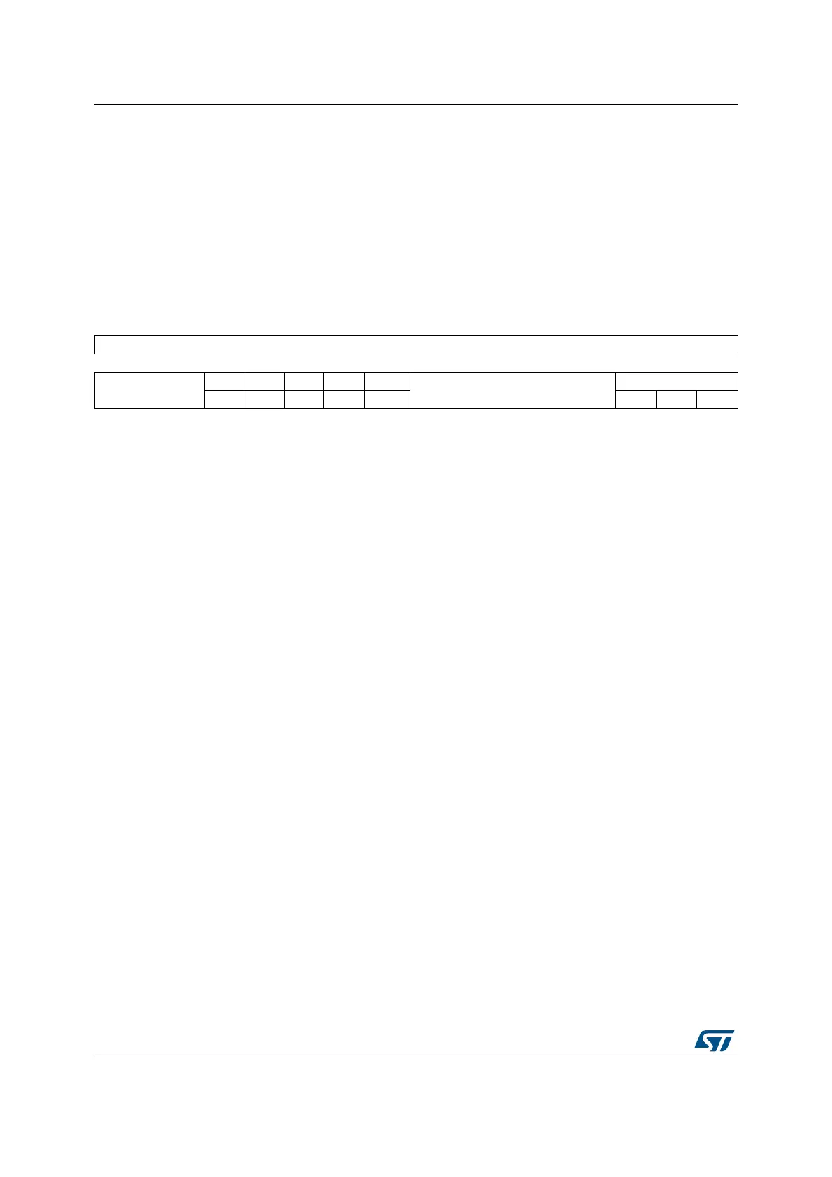
Address offset: 0x00
Reset value: 0x0000 0000
Access: no wait state, word, half-word and byte access
31 30 29 28 27 26 25 24 23 22 21 20 19 18 17 16
Reserved
15 14 13 12 11 10 9 8 7 6 5 4 3 2 1 0
Reserved
DCRST ICRST DCEN ICEN PRFTEN
Reserved
LATENCY
rwwrwrw rw rwrwrw
Bits 31:11 Reserved, must be kept cleared.
Bit 12 DCRST: Data cache reset
0: Data cache is not reset
1: Data cache is reset
This bit can be written only when the D cache is disabled.
Bit 11 ICRST: Instruction cache reset
0: Instruction cache is not reset
1: Instruction cache is reset
This bit can be written only when the I cache is disabled.
Bit 10 DCEN: Data cache enable
0: Data cache is disabled
1: Data cache is enabled
Bit 9 ICEN: Instruction cache enable
0: Instruction cache is disabled
1: Instruction cache is enabled
Bit 8 PRFTEN: Prefetch enable
0: Prefetch is disabled
1: Prefetch is enabled
Bits 7:3 Reserved, must be kept cleared.
Bits 2:0 LATENCY: Latency
These bits represent the ratio of the CPU clock period to the Flash memory access time.
000: Zero wait state
001: One wait state
010: Two wait states
011: Three wait states
100: Four wait states
101: Five wait states
110: Six wait states
111: Seven wait states
 Loading...


