DocID15687 Rev 5 19/29
PM0059 Flash memory interface
28
Write protection error flag
If an erase/program operation to a write protected area of the Flash memory is performed,
the Write Protection Error flag (WRPERR) is set in the FLASH_SR register.
If an erase operation is requested, the WRPERR bit is set when:
• Mass or sector erase are configured (MER or MER/MER1 and SER = 1)
• A sector erase is requested and the Sector Number SNB field is not valid
• A mass erase is requested while at least one of the user sector is write protected by
option bit (MER or MER/MER1 = 1 and nWRPi = 0 with 0 ≤ i ≤ 11 bits in the
FLASH_OPTCRx register
• The Flash memory is readout protected and an intrusion is detected.
If a program operation is requested, the WRPERR bit is set when:
• A write operation is performed on system memory or on the reserved part of the user
specific sector.
• A write operation is performed to the user configuration sector
• A write operation is performed on a sector write protected by option bit.
• A write operation is requested on an OTP area which is already locked
• The Flash memory is read protected and an intrusion is detected.
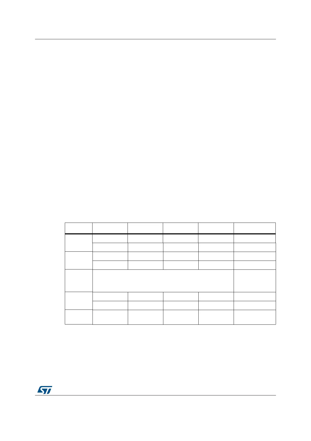
2.7 One-time programmable bytes
Table 9 shows the organization of the one-time programmable (OTP) part of the OTP area.
The OTP area is divided into 16 OTP data blocks of 32 bytes and one lock OTP block of 16
bytes. The OTP data and lock blocks cannot be erased. The lock block contains 16 bytes
LOCKBi (0 ≤ i ≤ 15) to lock the corresponding OTP data block (blocks 0 to 15). Each OTP
data block can be programmed until the value 0x00 is programmed in the corresponding
OTP lock byte. The lock bytes must only contain 0x00 and 0xFF values, otherwise the OTP
bytes might not be taken into account correctly.
Table 9. OTP part organization
Block [128:96] [95:64] [63:32] [31:0] Address byte 0
0
OTP0 OTP0 OTP0 OTP0 0x1FFF 7800
OTP0 OTP0 OTP0 OTP0 0x1FFF 7810
1
OTP1 OTP1 OTP1 OTP1 0x1FFF 7820
OTP1 OTP1 OTP1 OTP1 0x1FFF 7830
.
.
.
.
.
.
.
.
.
15
OTP15 OTP15 OTP15 OTP15 0x1FFF 79E0
OTP15 OTP15 OTP15 OTP15 0x1FFF 79F0
Lock block
LOCKB15 ...
LOCKB12
LOCKB11 ...
LOCKB8
LOCKB7 ...
LOCKB4
LOCKB3 ...
LOCKB0
0x1FFF 7A00
 Loading...


