6 STM32H7x7I-EVAL hardware layout and configuration
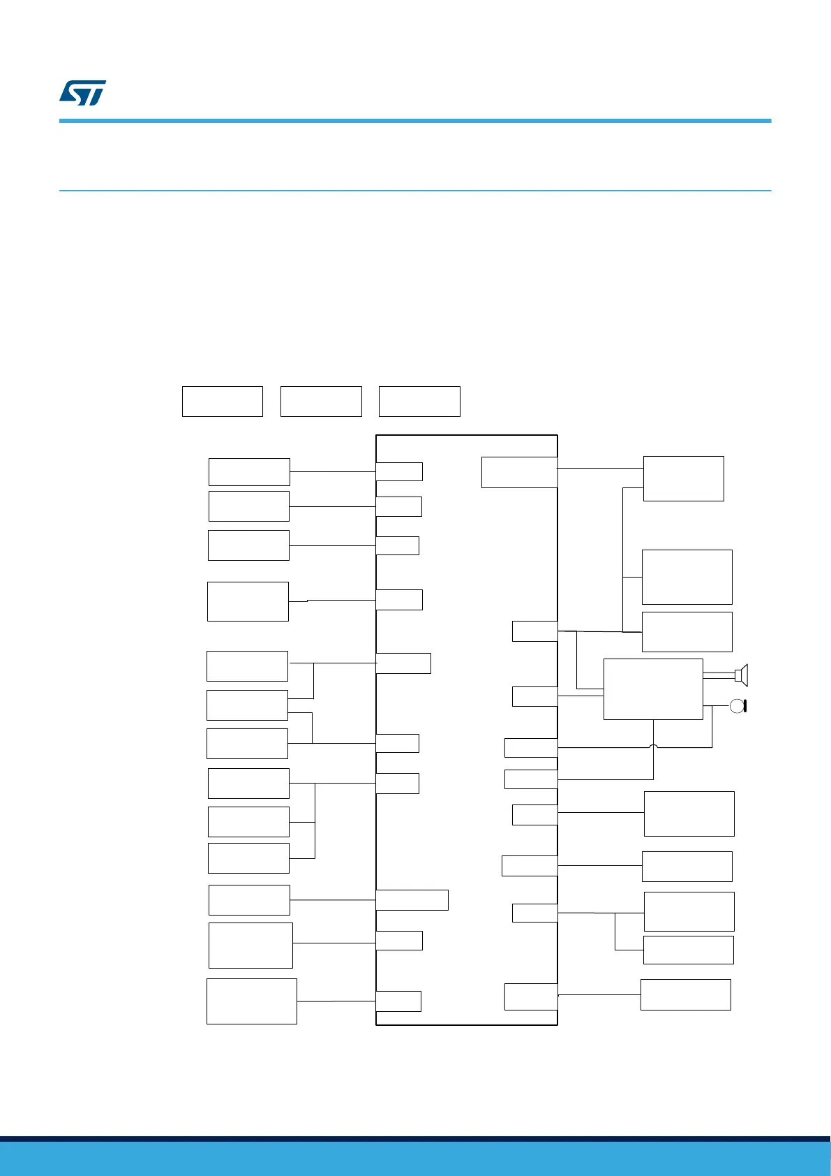
The STM32H7x7I-EVAL Evaluation boards are designed around the STM32H7x7XIH6U (240+25-pin TFBGA
package) microcontroller. Figure 2 shows the hardware block diagram for STM32H7x7XIH6U and illustrates the
connection between the microcontroller and the peripherals (SDRAM, SRAM, NOR Flash, Twin Quad-SPI Flash,
color LCD, USB OTG connectors, USART, Ethernet, Audio, FDCAN, microSD 3.0 card and embedded ST-LINK).
Figure 3. STM32H7x7I-EVAL Evaluation board (top side) helps users to locate these features on the Evaluation
board. The mechanical dimensions of the board are showed in Figure 4. STM32H7x7I-EVAL Evaluation board
mechanical drawing .
Figure 2. Hardware block diagram
STM32H7x7XIH6U
3V Battery
RTC
PHY &
Ethernet
connector
JTAG & trace
connector
DAP
1 RS232 DB9
connector
32 KHz
Crystal
VBAT
STLINK-V3E
I2C
USB connector
SW & trace
connector
TPIU
RMII
I2C connector
4" DSI LCD
MFX
Joystick and
LED
microSD card
CAN connector
FDCAN
Key, Wakeup &
Tamper buttons
GPIO
ADC
SDMMC 3.0
HS PHY & USB
connector
OTG1
NOR Flash
memory
SRAM
FMC
SDRAM
QSPI
1Gb/
2x512Mb
Twin QSPI
Flash
memory(ies)
OTG2
FS
USB connector
UART1
MIPI DSI
DFSDM
PDM
3.3V Power
supply
1.8V Power
supply
2.9V SD3.0
Power supply
Potentiometer
SAI1
Audio DAC &
amplifier
UM2525
STM32H7x7I-EVAL hardware layout and configuration
UM2525 - Rev 3
page 7/69