UM1574 Hardware and layout
Doc ID 023645 Rev 1 21/48
4.2.5 STM8AF board jumpers selection
4.2.6 STM8AF board extension connection
Male headers P1, P2 and P3 connectors can connect the STM8AF board to a standard
prototyping/wrapping board. Free GPI/Os of the STM8AF5288T are available on P1 and P2.
L99PM62GXP device I/Os are connected to P3. P1, P2 and P3 can also be probed by an
oscilloscope, a logic analyzer or a voltmeter.
P1 connector contains the full port B GPI/Os and the alternate functions are the first 8 ADC
channel inputs. Its standard HE10 format complies with some additional modules or
resources that are pin-to-pin equivalent.
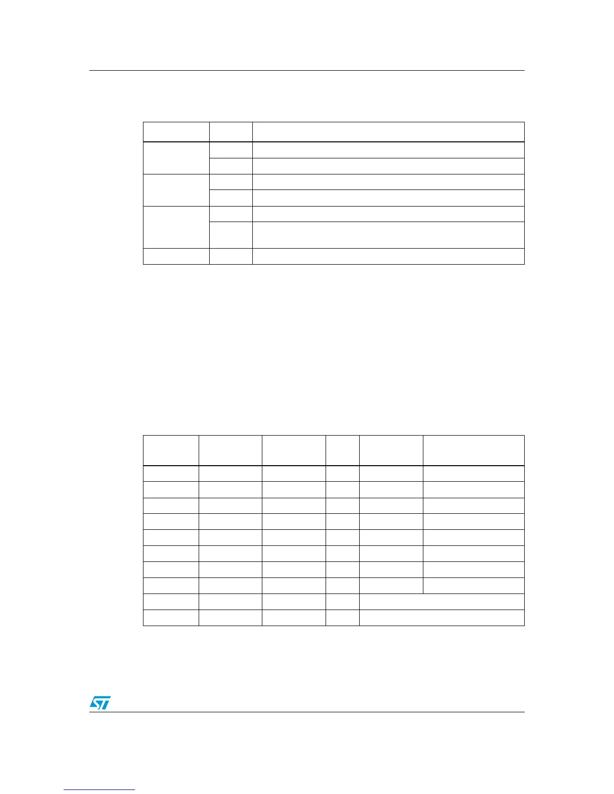
Table 3. STM8AF board jumper selection
Jumper State
(1)
1. Default jumper state is shown in bold.
Description
JP1
(LIN/FLASH)
1-2 Flash mode selected
(2)
.
2. The Flash mode is activated if at least JP1 or JP2 selects Flash mode.
2-3 LIN communication enabled.
JP2
(CAN/FLASH)
1-2 Flash mode selected
(2)
.
2-3 CAN communication enabled.
JP3 (I
DD
)
ON Standard operation, 5 V connected to the V
DD
of the microcontroller.
OFF
An ammeter can be connected between JP3 pins to measure the
current sunk by the MCU.
JP4 (Reserved) OFF Reserved, do not modify.
Table 4. STM8AF board P1 pinout microcontroller connectivity
Pin number
P1
Pin number
STM8AF MCU
Board pin
name
Type Main function Alternate function
1 22 PB0 I/O Port B0 Analog input AIN0
2 21 PB1 I/O Port B1 Analog input AIN1
3 20 PB2 I/O Port B2 Analog input AIN2
4 19 PB3 I/O Port B3 Analog input AIN3
5 18 PB4 I/O Port B4 Analog input AIN4
6 17 PB5 I/O Port B5 Analog input AIN5
7 16 PB6 I/O Port B6 Analog input AIN6
8 15 PB7 I/O Port B7 Analog input AIN7
9V
DD
Microcontroller Digital power supply
10 GND Digital ground