Analog-to-digital converter (ADC) AN2752
10/40 AN2752 Rev 6
3 Analog-to-digital converter (ADC)
3.1 Analog power
The ADC has an independent, analog supply reference voltage, isolated on input pin V
DDA
,
which allows the ADC to be supplied by a very clean voltage source. This analog voltage
supply range is the same as the digital voltage supply range on pin V
DD
. An isolated analog
supply ground connection on pin V
SSA
provides further ADC supply isolation. Together, the
analog supply voltage and analog supply ground connection, offer a separate external
analog reference voltage input for the ADC unit on the V
REF+
pin. This gives better accuracy
on low voltage input as follows:
• V
REF+
(input, analog reference positive): the higher/positive reference voltage for the
ADC needs to be between 250 mV and V
DDA
. For more details about V
REF+
values
refer to the STM8S or STM8AF datasheets. This input is bonded to V
DDA
in devices
that have no external V
REF+
pin (packages with 48 pins or less).
• V
REF-
(input, analog reference negative): the lower/negative reference voltage for the
ADC has to be higher than V
SSA
. For more details about V
REF-
values refer to the
STM8S or STM8AF datasheets. This input is bonded to V
SSA
in devices that have no
external V
REF-
pin (packages with 48 pins or less).
3.2 Analog input
STM8S and STM8AF devices have 16 analog input channels, which are converted by the
ADC one at a time, and each of them is multiplexed with an I/O.
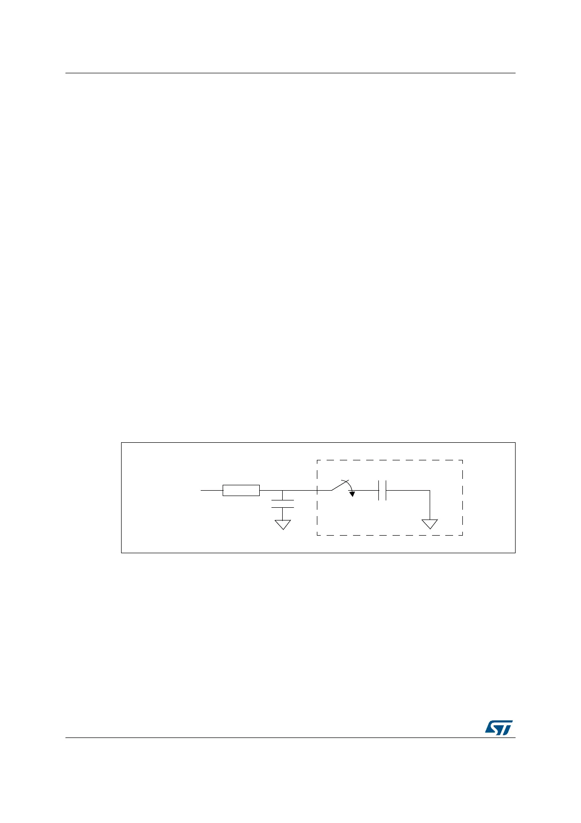
The analog input interface of the ADC is shown in Figure 4.
Figure 4. Analog input interface
V
IN_EXT
R
EXT
C
EXT
C
SAMP
SW
SAMP
V
IN
Outside ADC Inside ADC

 Loading...


