AN2752 Rev 6 9/40
AN2752 Power supply
39
Recommendations
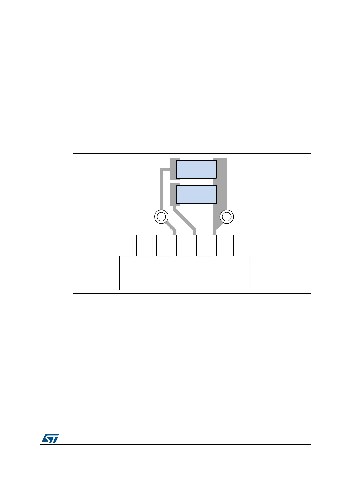
All pins need to be properly connected to the power supplies. It is important to have the
lowest possible impedance for these connections, including pads, tracks and vias. This is
typically achieved with thick track widths and dedicated power supply planes in multi-layer
printed circuit boards (PCBs).
In addition, each power supply pair has to be decoupled with 100 nF filtering ceramic
capacitors (C) with one chemical capacitor (1 to 2 µF) in parallel on the STM8S or STM8AF
device. The ceramic capacitors (including C
EXT
capacitor between VCAP and VSS pins)
need to be placed as close as possible or below the appropriate pins, on the opposite side
of the PCB. Typical values are 10 nF to 100 nF, but exact values depend on the application
needs.
Figure 3 shows the typical layout of the V
DD
/V
SS
and V
CAP
/V
SS
pairs.
Figure 3. Typical layout of V
DD
/V
SS
and V
CAP
/V
SS
pairs
069
9'' 9&$3 966
0&8
YLDWR9
''
YLDWR9
66
&
(;7
&

 Loading...


