Reset control AN2752
14/40 AN2752 Rev 6
5 Reset control
5.1 Reset management overview
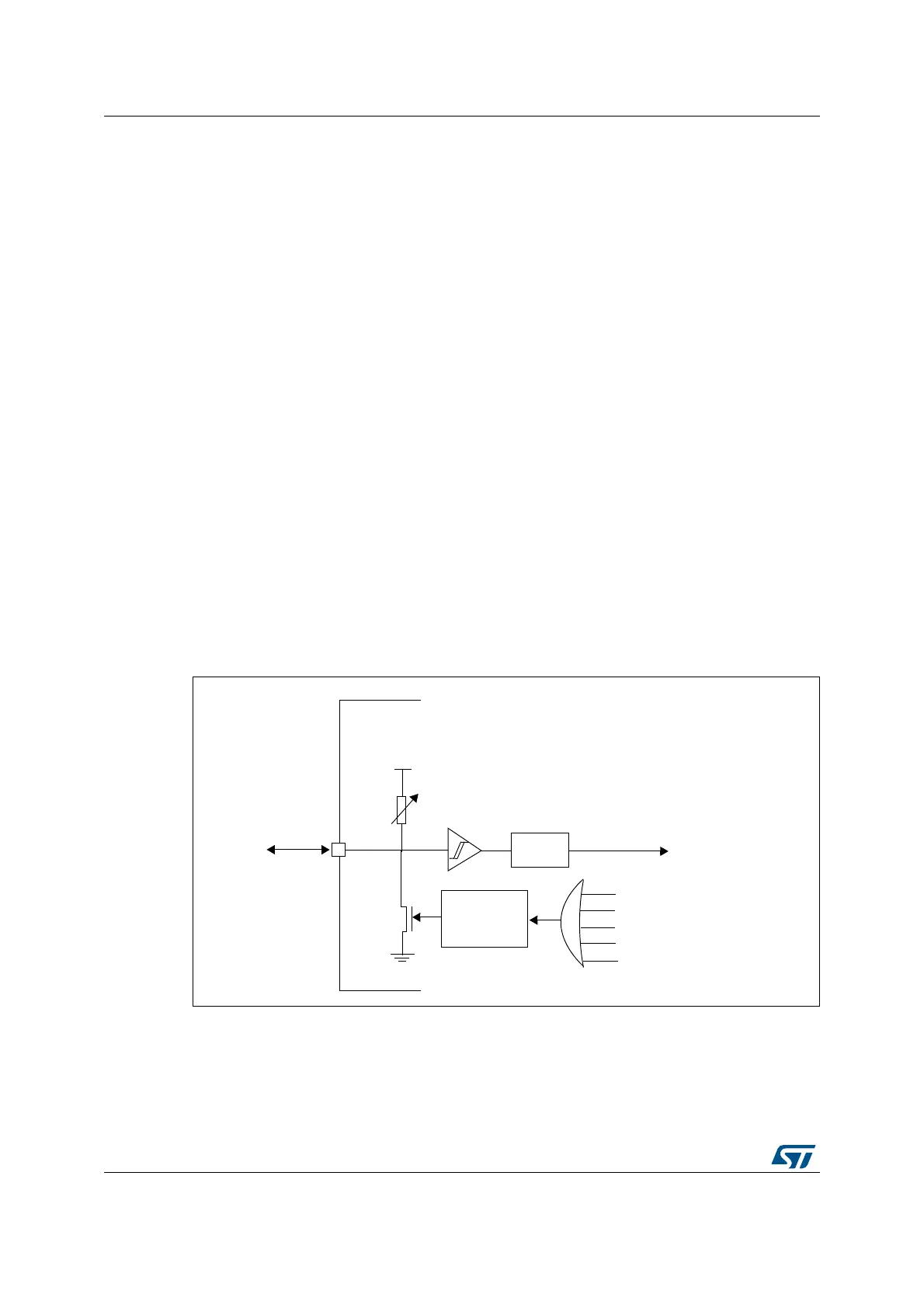
The reset cell is a dedicated 5 V bidirectional I/O. Its output buffer driving capability is fixed
to Io
MIN
= 2 mA at 0.4 V in the 3 V to 5.5 V range, which includes a 40 kΩ pull-up. Output
buffer is reduced to the n-channel MOSFET (NMOS). If a 40 kΩ pull-up is accepted, this cell
does not include an output buffer of 5 V capability. The receiver includes a glitch filter,
whereas the output buffer includes a 20 µs delay.
There are many reset sources, including:
• External reset through the NRST pin
• Power-on reset (POR) and brown-out reset (BOR): during power-on, the POR keeps
the device under reset until the supply voltage (V
DD
and V
DDIO
) reach the voltage level
at which the BOR starts to function.
• Independent watchdog reset (IWDG)
• Window watchdog reset (WWDG)
• Software reset: the application software can trigger reset
• SWIM reset: an external device connected to the SWIM interface can request the
SWIM block to generate a microcontroller reset
• Illegal opcode reset: if a code to be executed does not correspond to any opcode or
prebyte value, a reset is generated
• Electromagnetic susceptibility (EMS) reset: generated if critical registers are corrupted
or badly loaded
Figure 7. Reset management
STM8
Filter
Illegal op code reset
SWIM reset
EMS reset
POR/BOR reset
Delay
VDD_IO
System reset
NRST
External reset
R
PU
IWDG/WWDG/software reset
Pulse generator
(min 20 µs
Simplified functional I/O reset schematic

 Loading...


