AN2752 Rev 6 7/40
AN2752 Power supply
39
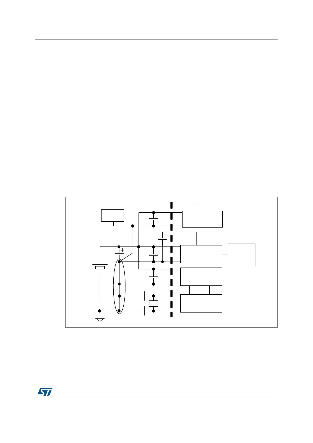
2 Power supply
2.1 Power supply overview
The device can be supplied through a 3.0 V to 5.5 V external source. An on-chip power
management system provides the 1.8 V digital supply to the core logic, both in normal and
low power modes. It is also capable of detecting voltage drops, on both external
(3.3
V / 5 V) and internal (1.8 V) supplies.
The device provides:
• one pair of pads V
DD
/V
SS
(3.3 V ± 0.3 V to 5 V ± 0.5 V) dedicated to the main regulator
ballast transistor supply.
• two pairs of pads dedicated for V
DD_IO
/V
SS_IO
(3.3 V ± 0.3 V to 5 V ± 0.5 V), which are
used to power only the I/O’s. On 32-pin packages, only one pair is bonded.
Note: For V
DDIO
/V
SSIO
next to V
DD
/V
SS
, it is recommended to connect these two pairs together
and to use only a decoupling capacitor. The purpose is to ensure good noise immunity by
reducing the connection length between both supplies and also between V
DD
/V
DDIO
and the
capacitor.
• One pair of pads V
DDA
/V
SSA
(3.3 V ± 0.3 V to 5 V ± 0.5 V) dedicated to analog
functions. Refer to Section 3: Analog-to-digital converter (ADC) for more details.
Figure 1. Power supply
Note: The capacitors must be connected as close as possible to the device supplies (especially
V
DD
in case of dedicated ground plane).
Placing a crystal/resonator on OSCIN/OSCOUT is optional. The resonator must be
connected as close as possible to the OSCIN and OSCOUT pins. The loading capacitance
ground must be connected as close as possible to V
SS
.
Main / Low power
regulator
CPU
RAM
Logic
Analog functions
IOsIOs
XTAL
Star connected
Analog
signal
V
CAP
VDD/VDDIO1
VDDIO2
V
SSIO2
V
DDA
V
SSA
OSCIN
OSCOUT
V
DDIO
V
SSIO
V
SSIO
V
DDIO
3.3V - 5V

 Loading...


