Chapter 2: Installation
2-25
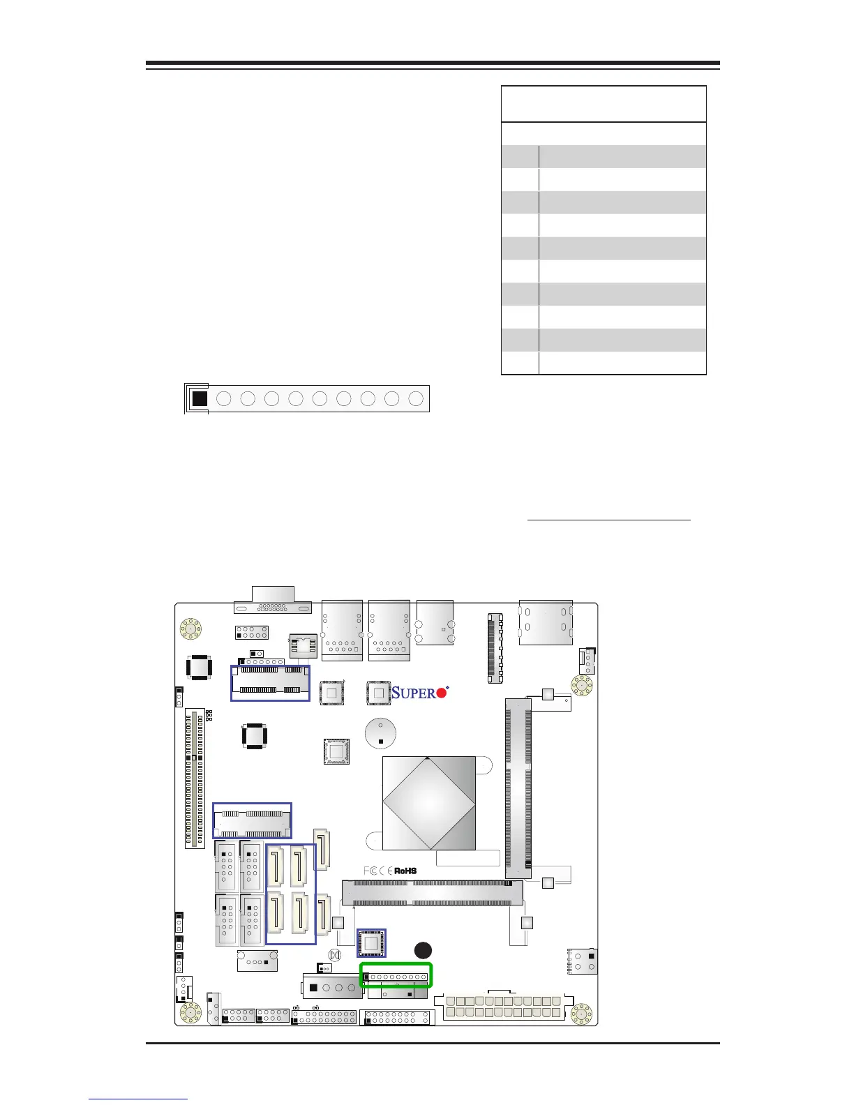
X10SBA(-L)
Rev.
1.01A
JSMB1
J31
JBT1
BT2
M-SATA0M-SATA1
M-SATA2
M-SATA3
JP1
LAN1LAN2
JDIMM2
PJ1
JF1
JTPM1
JOH1
JSPDIF_OUT
JPUSB1
JPAC1
JPME2
JD1
VGA
FAN1
FAN2
I-SATA1
COM4
COM2
SP1
JSD1
JDIMM1
LED3
LED4
LED2
JPW1
SMBUS1
SLOT1 PCI-E 2.0 X2 (IN X8)
USB4/5
USB6
AUDIO FP
SODIMM2 (1.35V only)
USB1(2.0)
USB0(3.0)
CPU
(Install first)SODIMM1(1.35V only)
eDP
Non-ECC DDR3 Required
HDMI/DP
COM3
FP CTRL
BIOS
BAR CODE
J1
(for mini-PCI-E only)
(for M-SATA only)
J2
COM1
(for X10SBA only)
(for X10SBA only)
(for X10SBA only)
(for X10SBA)
LED1
LED5
USB2/3
I-SATA0
GPIO Header (JP1)
The JP1 header is located near the
onbaord battery on the motherboard.
JP1 is a 10-pin general purpose I/O
header. Each pin can be congured to
be an input pin or open drain output
pin. See the table on the right for pin
denitions.
General Purpose I/O Header
Pin Denitions
Pin# Denition
1 +3.3V
2 SOC_P3V3_GPIO_S5_31
3 SOC_P3V3_GPIO_S5_32
4 SOC_P3V3_GPIO_S5_33
5 SOC_P3V3_GPIO_S5_34
6 SOC_P3V3_GPIO_S5_35
7 SOC_P3V3_GPIO_S5_36
8 SOC_P3V3_GPIO_S5_37
9 SOC_P3V3_GPIO_S5_38
10 GND
A
A. General Purpose Header