13
Chapter 1: Introduction
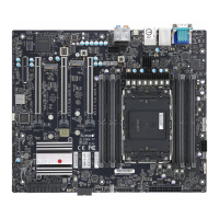
Figure 1-4. Motherboard Layout
Notes:
• " " indicates the location of pin 1.
• Jumpers/components/LED indicators not indicated are used for internal testing only.
1.5 Motherboard Layout
See the table on the following page for descriptions. For detailed descriptions, pinout
DESIGNED IN USA
H12DSG-O-CPU
REV:1.01
1 2 3
BIOS LICENSE
BAR CODE
IPMI CODE
BT1
JNCSI1
CPU1CPU2
BP-PWR3
BP-PWR2
BP-PWR1
JBT1
FAN1FAN3FAN4
FAN5FAN6FAN7FAN8
FAN10
JF1
JOH1
JPW2JPW1
STDY-PWRA
JTPM1
I-SATA0~3
JIPMB1
P1-PCIE5B/NVMe
P1-PCIE5A/NVMe
GPU-PWR6 ~ GPU-PWR10
GPU-PWR1 ~ GPU-PWR5
P2-DIMMD2~P2-DIMMA1
P2-DIMME1~P2-DIMMH2
P1-DIMME1~P2-DIMMH2
P1-DIMMD2~P1-DIMMA1
JSLIM-RA1
JSLIM-RA2
FAN2
USB3/4 (2.0)
P2-PCIE10B/NVMe
P2-PCIE10A/NVMe
JL1
AIOM
JPW3 JPW4
JSLOT1
FAN9
P2-PCIE7A/NVMe
P2-PCIE7B/NVMe
P2-PCIE6B/NVMe
P2-PCIE6A/NVMe
P2-PCIE8A
P2-PCIE8B
P2-PCIE9A
P2-PCIE9B
P1-PCIE1A
P1-PCIE1B
P1-PCIE2A
P1-PCIE2B
P1-PCIE3A/NVMe
P1-PCIE4B/NVMe
P1-PCIE4A/NVMe
P1-PCIE3B/NVMe
JPFR3
JWD1
JPFR1
LED2
LED6
 Loading...