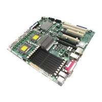
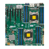
2-10
X7DCU User's Manual
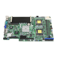
LE2
SW1
JD1
JBT1
JWOR1
JL1
JOH1
JCF1
JK1
JPEW2
JP6
JP7
JPL1
JWD1
JIDE
FAN6
FAN5
FAN7
JWF1
I-SATA0
CPU2
CPU1
SXB2:PCI-E X8
UIOP
BANK3
JWOL
SGPIO2
SGPIO1
COM2
CPU FAN1
KB/MS
SMBUS_PS
COM1
USB0/1
BANK2
LAN1
VGA
BANK1
DIMM1C
DIMM2B
DIMM1A
DIMM1B
DIMM2A
LAN2
CPU FAN2
Compact Flash
IDE
Floppy
SXB1:PCI-E X16
USB 4
USB 2/3
JPEW1
Battery
DIMM2C
SIMSO IPMI
VGA CTRL
LAN CTRL
Intel 5100
North Bridge
Intel ICH9R
South Bridge
USB5
LE19
X7DCU
S I/O
I-SATA1
I-SATA2
I-SATA3
I-SATA4
I-SATA5
Buzzer
JF1
JPW1
JPW2
JPW3
FAN1
FAN2
FAN3
FAN8
FAN4
JPG1
Power LED
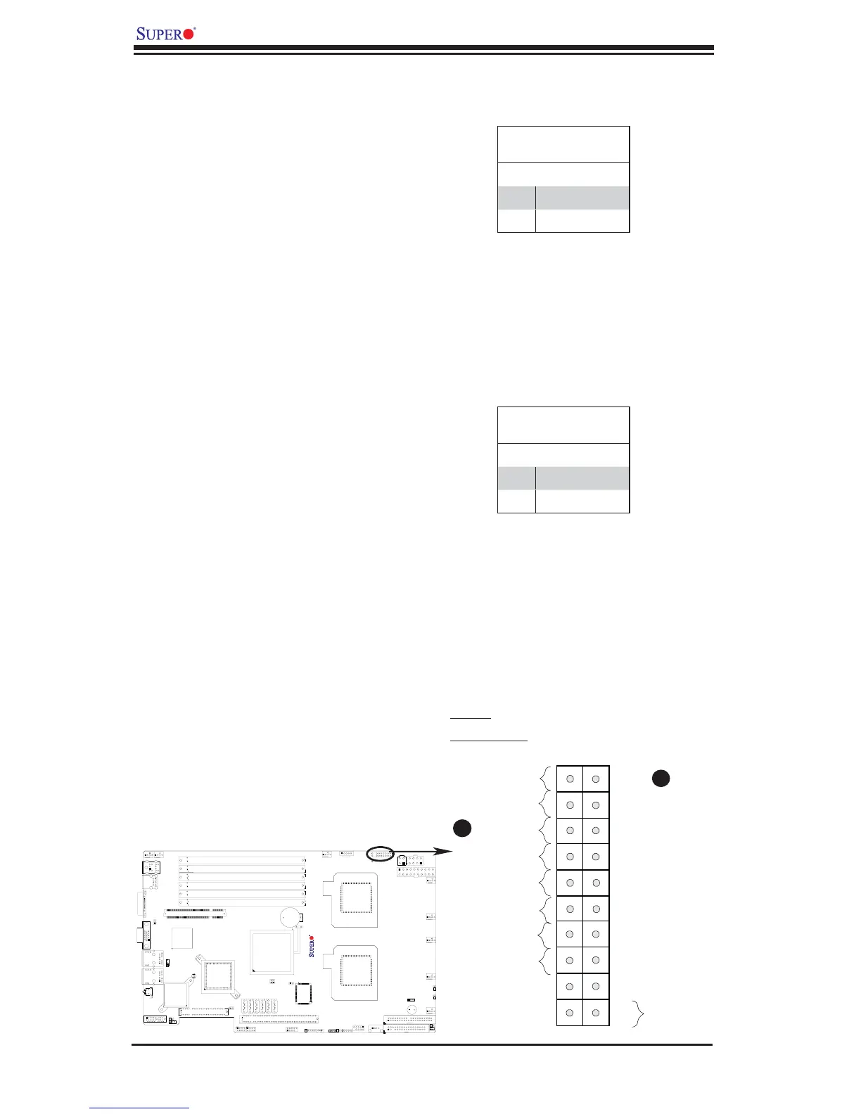
The Power LED connection is located
on pins 15 and 16 of JF1. Refer to the
table on the right for pin defi nitions.
NMI Button
The non-maskable interrupt button
header is located on pins 19 and 20
of JF1. Refer to the table on the right
for pin defi nitions.
FP Power
OH/Fan Fail/
PWR Fail/UID LED
1
NIC1 LED
FP Reset B
2
HDD LED
Power LED
Reset
PWR
Vcc
UID Switch/Vcc
Vcc
Blue_LED_Cath
(UID)/Vcc
Ground
Ground
1920
Vcc
X
Ground
NMI
X
Vcc
PWR Fail LED
NIC2 LED
NMI Button
Pin Defi nitions (JF1)
Pin# Defi nition
19 Control
20 Ground
Power LED
Pin Defi nitions (JF1)
Pin# Defi nition
15 +5V
16 Ground
Front Control Panel Pin Defi nitions
A. NMI
B. PWR LED
A
B