Chapter 2: Installation
2-15
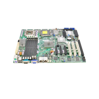
LE2
SW1
JD1
JBT1
JWOR1
JL1
JOH1
JCF1
JK1
JPEW2
JP6
JP7
JPL1
JWD1
JIDE
FAN6
FAN5
FAN7
I-SATA0
CPU2
CPU1
SXB2:PCI-E X8
UIOP
BANK3
JWOL
SGPIO2
SGPIO1
COM2
CPU FAN1
KB/MS
SMBUS_PS
COM1
USB0/1
BANK2
LAN1
VGA
BANK1
DIMM1C
DIMM2B
DIMM1A
DIMM1B
DIMM2A
LAN2
CPU FAN2
Compact Flash
IDE
SXB1:PCI-E X16
USB 4
USB 2/3
JPEW1
Battery
DIMM2C
SIMSO IPMI
VGA CTRL
LAN CTRL
Intel 5100
North Bridge
Intel ICH9R
South Bridge
USB5
LE19
X7DCU
S I/O
I-SATA1
I-SATA2
I-SATA3
I-SATA4
I-SATA5
Buzzer
JF1
JPW1
JPW2
JPW3
FAN1
FAN2
FAN3
FAN8
FAN4
JPG1
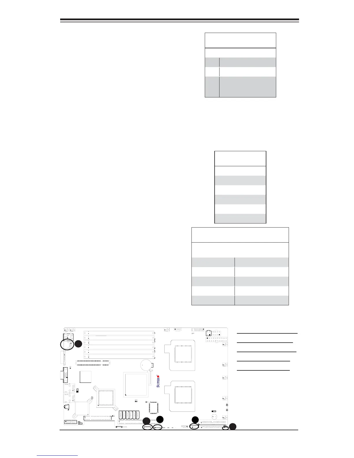
Universal Serial Bus (USB)
There are six USB 2.0 (Universal
Serial Bus) ports/headers on the
motherboard. Two of them are Back
Panel USB ports: USB 0~1 (JPUSB1).
The other four are Front Panel USB
connectors: USB 2~3 (JUSB2), USB
4 (JUSB3), and USB 5 (JUSB 4).
See the tables on the right for pin
defi nitions.
A
B
C
A. Compact Flash Power
B. Backpanel USB 0~1
C. Front Panel USB 2~3
D. Front Panel USB 4
E. Front Panel USB 5
Back Panel USB
(USB 0~1)
Pin# Defi nitions
1 +5V
2 PO-
3 PO+
4 Ground
5 N/A
Front Panel USB
Pin Defi nitions (USB 2~5)
USB 2/4
Pin # Defi nition
USB 3/5
Pin # Defi nition
1 +5V 1 +5V
2 PO- 2 PO-
3 PO+ 3 PO+
4 Ground 4 Ground
5 Key 5 No connection
Compact Flash Card Power
Connector
A Compact Flash card power con-
nector is located at JPWF1. For the
Compact Flash card to work properly,
you will need to connect a Compact
Flash card power cable to JPWF1
fi rst. Refer to the board layout below
for the location.
Compact Flash Card PWR
Connector Pin Defi nition
Pin# Defi nition
1 +5V
2 Ground
3 JCF1 Signal (JCF1:
Compact Flash Master/
Slave Select Jumper)