2-26
X9DRL-3F/X9DRL-iF Motherboard User’s Manual
Power Button
Blue+ (OH/Fan Fail/
PWR FaiL/UID LED)
1
NIC1 Link LED
Reset Button
2
Power Fail LED
HDD LED
FP PWRLED
Reset
PWR
3.3 V
ID_UID_SW/3/3V Stby
Red+ (Blue LED Cathode)
Ground
Ground
1920
3.3V
X
Ground
NMI
X
NIC2 Link LED
NIC2 Activity LED
NIC1 Activity LED
Power Fail LED
The Power Fail LED connection is
located on pins 5 and 6 of JF1. Re-
fer to the table on the right for pin
denitions.
A. OH/Fail/PWR Fail LED
B. PWR Supply Fail
PWR Fail LED
PinDenitions(JF1)
Pin# Denition
5 3.3V
6 PWR Supply Fail
B
A
Overheat (OH)/Fan Fail/PWR Fail/
UID LED
Connect an LED cable to pins 7 and
8 of Front Control Panel to use the
Overheat/Fan Fail/Power Fail and
UID LED connections. The Red LED
on pin 7 provides warnings of over-
heat, fan failure or power failure. The
Blue LED on pin 8 works as the front
panel UID LED indicator. The Red
LED takes precedence over the Blue
LED by default. Refer to the table on
the right for pin denitions.
OH/Fan Fail/ PWR Fail/Blue_UID
LEDPinDenitions(JF1)
Pin# Denition
7 Red_LED-Cathode/OH/Fan Fail/
Power Fail5.5V.SB
8 Blue_UID LED
OH/Fan Fail/PWR Fail
LED Status (Red LED)
State Denition
Off Normal
On Overheat
Flashing Fan Fail
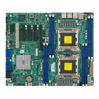
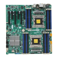
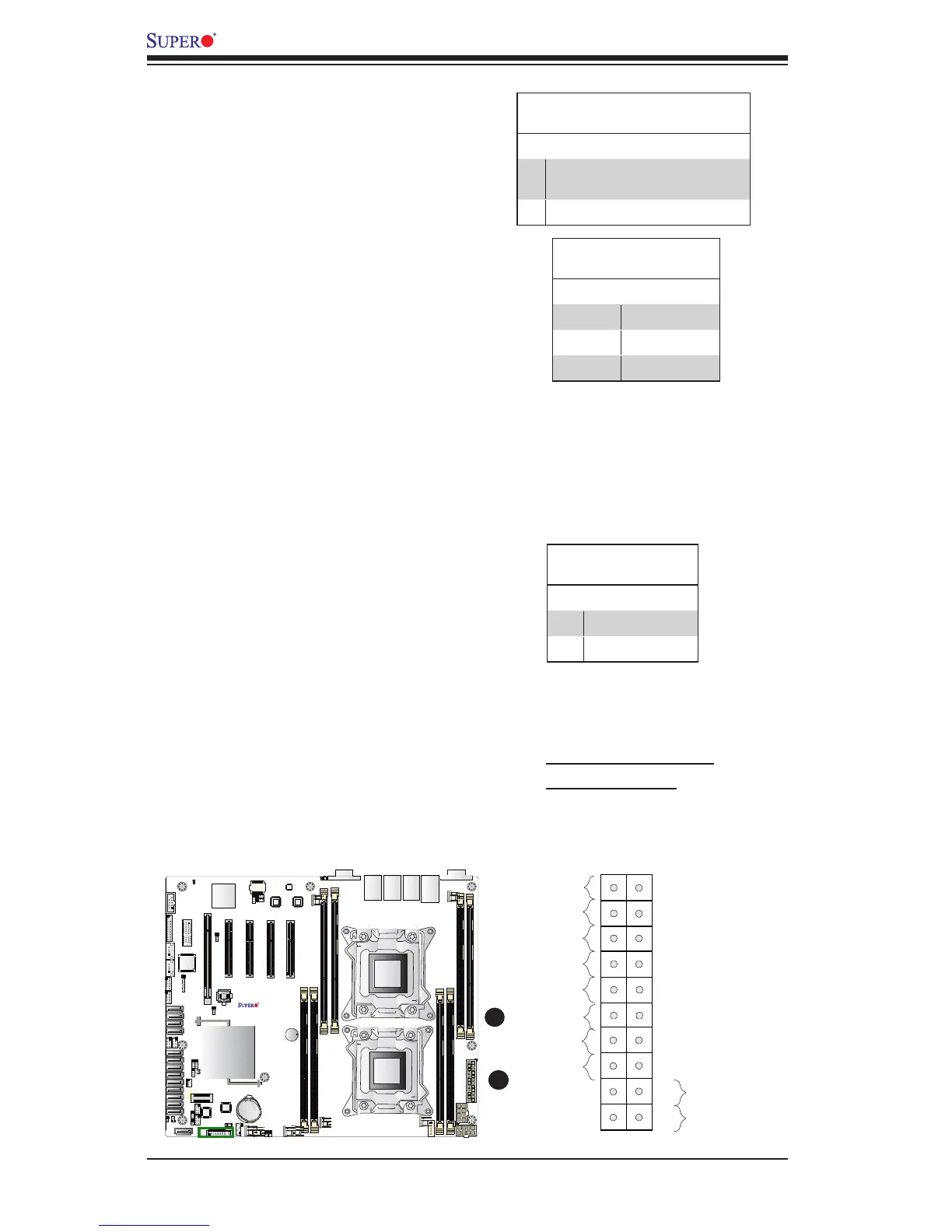
JSD1
P2-DIMMH1
P2-DIMMG1
P2-DIMMF1
P2-DIMME1
P1-DIMMD1
P1-DIMMC1
P1-DIMMB1
P1-DIMMA1
COM1
JPW4
JTPM1
LAN1LAN2
COM2
JPW1
JPW2
JPI2C1
JIPMB1
FAN3
FAN4
FAN1
FAN5
FAN2
FAN6
JPG1
JPB1
JWD1
JPME1
JWP1
JPL2
JPL1
LED2
LEDM1
JD1
JF1
6-SGPIO2
T-SGPIO1
I-SATA0
I-SATA1
SAS/SATA1
SAS/SATA2
SAS/SATA3
S-SAS4
S-SAS5
S-SAS6
S-SAS7
JL1
JI2C1
JI2C2
I-SATA2
I-SATA5
I-SATA4
I-SATA3
JBT1
JSTBY1
JRK1
UID
SLOT1 PCI-E 2.0 X1
USB0/1USB2/3
USB5
USB4
PCH
SLOT2 PCI 33MHZ
PCH SLOT3 PCI-E 2.0 X4 (IN X8)
CPU1 SLOT4 PCI-E 3.0 X8
CPU1 SLOT5 PCI-E 3.0 X8
CPU1 SLOT6 PCI-E 3.0 X8)
X9DRL-iF
Rev. 1.01
IPMI_LAN
BUZZER
KB/MOUSE
V
T
FANA
FANB
a
VGA
A
ah
USB8/9
CPU1
USB6/7
CPU2
6-SGPIO1
SAS/SATA0
Battery
JOH1
JP2
JPME2
LED1
JUIDB1
J9
JITP2
T-SGPIO2
BMC CTRL
BIOS
LAN CTRL
LAN CTRL
BMC Firmware
CPLD
Intel PCH
 Loading...