122
3-7.
MEMORY
CIRCUIT
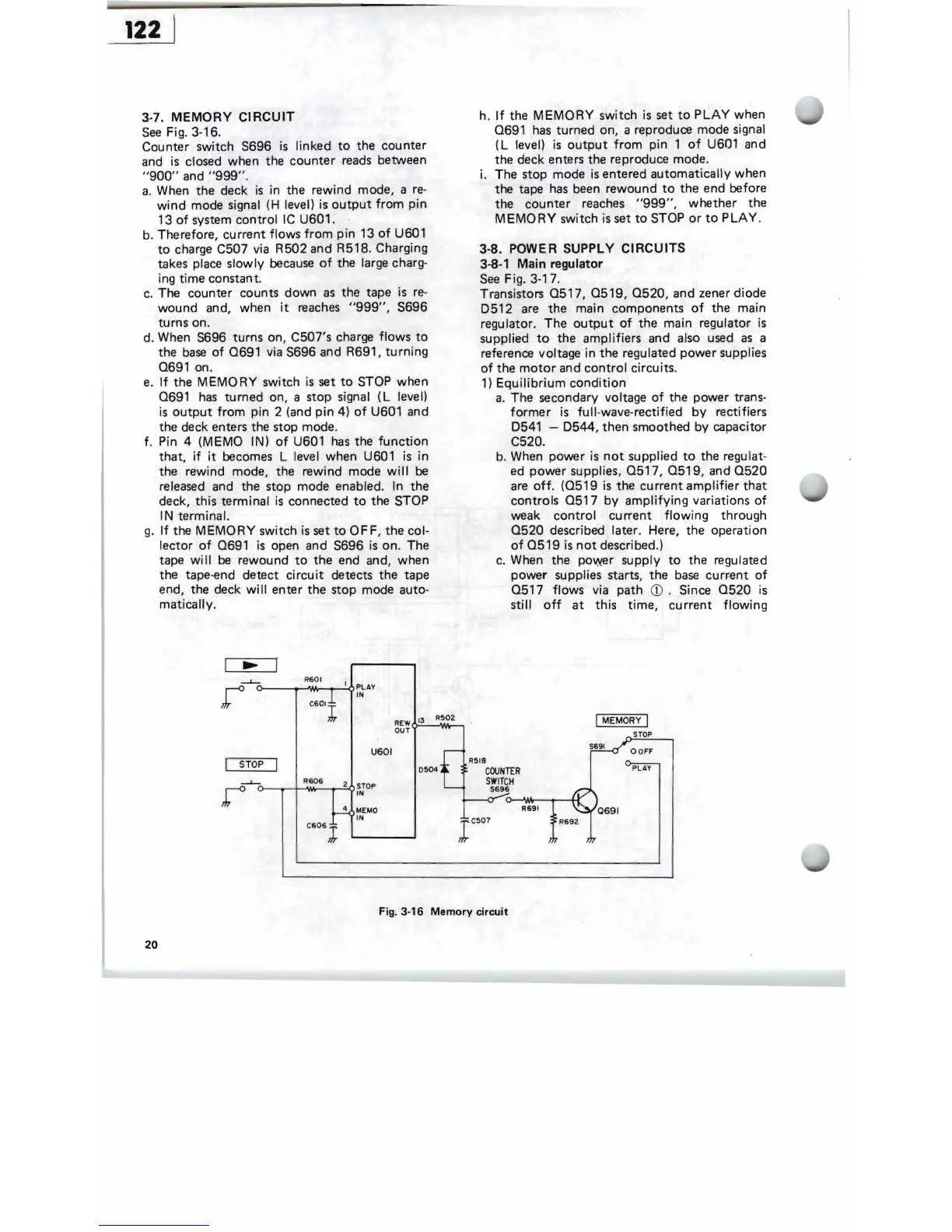
See
Fig. 3-16.
Counter switch S696
is
linked
to
the
counter
and
is
closed when the
counter
reads
between
"900"
and
"999".
a.
When the deck
is
in the rewind mode, a
re-
wind
mode signal
(H
level) is
output
from
pin
13
of
system
control
IC
U601.
b. Therefore, current flows
from
pin
13
of
U601
to
charge C507 via R502 and R518. Charging
takes place
slowly
because
of
the large charg-
ing time constant.
c.
The counter counts
down
as
the tape
is
re-
wound
and, when
it
reaches
"999",
S696
turns on.
d. When 5696 turns on, C507's charge
flows
to
the
base
of
0691
via S696 and R691,
turning
0691
on.
e.
If
the
MEMORY
switch
is
set
to
STOP when
0691
has
turned on, a stop signal
(L
level)
is
output
from
pin 2 (and
pin
4)
of
U601 and
the deck enters the stop mode.
f. Pin 4 (MEMO IN)
of
U601
has
the
function
that,
if
it
becomes L level when U601 is in
the rewind mode, the rewind mode
will
be
released and the stop mode enabled. In the
deck, this terminal
is
connected
to
the STOP
IN terminal.
g.
If
the
MEMORY
switch
is
set
to
OFF,
the col-
lector
of
0691
is
open and S696
is
on. The
tape
will
be
rewound
to
the end and, when
the tape-end detect
circuit
detects the tape
end, the deck
wi
II
enter the stop mode auto-
matically.
•
~
R601
r
C60l
I
I- STOP
R606
r
~
2
4
C606;;;
PLAY
IN
REW
13
OUT
U601
R502
0504
STOP
IN
MEMO
IN
r
C507
h.
If
the
MEMORY
switch
is
set
to
PLAY
when
0691
has
turned on, a reproduce mode signal
(L
level)
is
output
from
pin 1
of
U601 and
the deck enters the reproduce mode.
i. The stop mode
is
entered
automatically
when
the tape
has
been rewound
to
the end before
the
counter
reaches
"999",
whether
the
MEMORY
switch
is
set
to
STOP
or
to
PLAY
.
3-8. POWER SUPPLY
CIRCUITS
3-8-1 Main regulator
See
Fig. 3-17.
Transistors
0517, 0519,
0520,
and zener diode
D512
are
the main components
of
the main
regulator. The
output
of
the
main regulator
is
supplied
to
the amplifiers and also used
as
a
reference voltage in the regulated
power
supplies
of
the
motor
and
control
circuits.
1)
Equilibrium
condition
a.
The secondary voltage
of
the power trans-
former
is
full-wave-rectified
by
rectifiers
D541 -
D544,
then smoothed by capacitor
C520.
b. When power is
not
supplied
to
the regulat-
ed
power
supplies,
0517,
0519,
and
0520
are
off
.
(0519
is
the
currentamp
ll
ifierthat
controls
0517
by
amplifying
variations
of
weak
control
current
flowing
through
0520
described later. Here, the operation
of
0519
is
not
described.)
c.
When the
po~er
supply
to
the regulated
power supplies starts, the
base
current
of
0517
flows via path
CD
. Since
0520
is
still
off
at
this
time,
current
flowing
I
MEMORY
I
STOP
S691
OOFF
PLAY
069
1
Fig. 3-16
Memory
circuit
20


 To Next Page