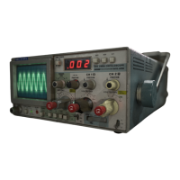
Theory
of
Operation-213
Service
In
the Oscilloscope function the input signal
is
further am-
plified
by
the Scope Preamplifier, which provides vertical
gain switching, variable gain control,
and
positioning. The
resultant signal drives the Vertical Output Amplifier which
causes vertical crt deflection to create a display.
The
Sweep
Generator
produces
a linear
sawtooth
sweep
sig-
nal
for
horizontal
deflection.
It
is
triggered
internally
from
a
portion
of
the
vertical
input
signal,
externally
from
a se-
parate
trigger
source,
or
free-runs
in
an internal ac
automa
-
tic
mode
of
operation
during
the
absence
of
an
adequate
internal
signal level.
The
output
of
the
sweep
generator
is
amplified
by
the
Horizontal
Output
Amplifier
which
causes
horizontal
crt
deflection
to
create
a linear sweep.
The
Sweep
Generator
also
generates
a signal
to
the
Z-Axis
Amplifier
for
display
blanking
and
unblanking.
All
voltages
required
to
operate
the
instrument
are provided
by
a
battery
operated
power
supply,
which
is
recharged
by
an integral
battery
charger
when
connected
to
the
power
line.
CIRCUIT
DESCRIPTION
Unless
otherwise
specified,
the
following
detailed
circuit
descriptions
will
make
reference
to
the
schematic
diagrams
in
the
Diagrams
section
at
the
rear
of
this
manual.
ATTENUATOR & INPUT AMPLIFIER
<v
The
input
section
consists
of
the
voltage
and
current-resis-
tance
inputs
and
input
switching; voltage
input
coupling
and
attenuation;
the
current
shunt
resistor
network;
the
Ohms
Converter;
and
the
Input
Buffer
Amplifier.
Input
Switching
Input
switching
is
accomplished
by
a
combination
of
physi-
cal
input
connections
and self-cancelling
pushbuttons.
Vol-
tage
inputs
are
made
from
the
probe
tip
through
probe
input
P100,
while
current
and resistance
inputs
are
made
through
J 120.
Switch
S 160 selects
the
type
of
input
(voltage, cur-
rent,
or
resistance);
connects
the
appropriate
voltage
atten-
uator,
current
shunt
resistor,
or
the
Ohms
Converter
with
its scaling resistor
network;
and
connects
the
selected
input
to
the
Buffer
Amp
I ifier.
Voltage Coupling and Attenuation
Voltage
inputs
from
P100
are
coupled
to
the
attenuator
through
INPUT
COUPLING
switch
S100.
In
the
DC posi-
tion
of
S100,
all signals
present
at
the
probe
enter
the
at-
tenuator.
In
the
AC
position,
the
de
signals are
blocked
by
C101
and
only
the
ac signals
enter.
In
the
GND
position
of
S100,
the
Buffer
Amplifier side
of
S100
is
grounded
to
provide
a
ground
reference
without
physically
disconnecting
the
probe
3-2
to
ground
it. In
this
position,
the
input
coupling
capacitor,
C
101,
is
precharged
through
R 101
to
ground.
The
signal
enters
the
attenuator
section and passes
through
without
attenuation
or
is
attenuated
by
1000:
1,
100:
1,
or
10: 1,
depending
upon
the
position
of
the
S120
switch
con-
tacts.
When
contact
18
is
open
and
16
is
closed,
10: 1
atten-
uation
is
provided
by
R
108,
R
109,
and
their
associated
series-parallel
components.
When
contact
21
is
open
and
19
is
closed,
100:
1
attenuation
is
provided by R
103,
R
106,
and
their
associated series-parallel
components.
When
both
contacts
18
and
21
are
open,
and
16
and
19
are closed,
1000:
1
attenuation
is
provided.
When 18 and 21 are closed,
and
16
and
19
are
open,
there
is
no
attenuation.
Resistor
pairs R 103-R
106
and
R 108-R
109
are precision
matched
pairs.
Capacitors
C104,
C108,
and
C112
provide
attenuator
frequency
compensation.
The
output
of
the
attenuator
is
connected
or
disconnected
from
the
Buffer
Amplifier
input
by
the
VOL
TS
section
of
S160.
Current Shunt Resistors
Current
inputs
are
connected
between
the
mA-Q
jack, J
120,
and
the
COMMON
jack,
J
125.
When
the
current
mode
is
selected
by
S160,
an
input
voltage
for
the
Buffer
Amplifier
is
generated
by
current
flow
through
combinations
of
resis-
tor
network
R
115,
R
117,
and R
118
as selected by S 12p.
Clamping
diodes
CR
118
through
CR 121 and fuse F 161 pro-
vide
input
protection
in
the
current
mode.
Ohms Converter
Figure 3-1
is
a
detailed
block
diagram
of
the
Ohms
Conver-
ter
circuitry.
Resistance
inputs
share
input
connectors
J120
and
J125
with
the
current
input.
When
S160
is
in
the
OHMS
mode,
a
constant
current
source
is
connected
to
J
120,
and
resis-
tance
is
measured
by
passing a
constant
current
through,
and measuring
the
voltage across
the
unknown
resistance.
This
measured
voltage,
which
is
directly
proportional
to
the
unknown
resistance,
becomes
the
input
voltage
to
the
Buf-
fer
Amplifier.
The
Ohms
Converter
circuit
consists
of
a precision
current
generator
0214
and
0215,
an
operational
amplifier
U175C,
and
the
range sealing resistors R
120
through
R
123.
U 175C
is
connected
to
the
feedback
summing
junction
of
the
Buffer
Amplifier;
therefore,
its inverting
and
non-inver-
ting
inputs
are
at
the
same
input
voltage as
the
input
of
the
Buffer
Amplifier.
The
precision
current
generator
provides
a
0.5
milliampere
current
(adjusted by
R215
during
calibra-
tion)
through
R165which
establishes and
maintains
a 1
volt
drop
across
that
resistor.
This
voltage
drop
keeps
the
output
of
U
175C
at
1
volt
more
negative
than
the
potential
at
J120,
which
is
the
input
to
the
Buffer
Ampl
ifier.
The
REV APR 1982
 Loading...