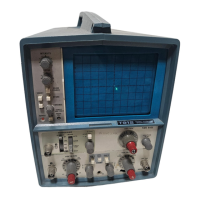
Options~T912
CIRCUIT
DESCRIPTION
Introduction
The following
paragraphs describe circuitry unique
to
Option 1, Refer to the Circuit Description
section of this
manual for a
description
of those portions of the circuitry
that
are unchanged by Option 1.
Note that
numbering of
the
terminals and sections
of
several integrated
circuits in
Option
1 differs from their counterparts in the
standard
instrument.
Refer
to the Option 1 schematic diagrams at the
back
of
the Diagrams section
of
this
manual
for circuitry discuss-
ed in this
circuit
description.
Digital Logic devices are used
to perform some of the
functions
in
this
instrument. LO and HI
designations
are
used in this circuit
description
to indicate the state
of
the
digital circuit. HI indicates the
more positive
of the two
levels. The specific
voltages
which constitute
LO and HI
logic states, may vary
between individual
devices.
Preamplifier
The buffer stages
Q4302 and
04303 isolate the channel
1
preamplifier
from the switching
diodes and from the
delay line
driver.
The
channel
2
preamplifier
is isolated
from the
switching diodes and the
delay line
driver by transistors
Q4310 and Q4311 or
transistors Q4312 and
04313.
For
a
normal
display (DIFF button
not
depressed), the
channel 2 signal is
passed through
Q4312 and
Q4313 to
the switching diodes.
Vertical
Mode switch
S4370 con-
nects approximately
+4.4 V from
R4302, R4303, and
R431
3
through
R431 2 to the bases of
Q431
2
and
04313. At
the same time,
+8
V is connected
to
04310 and Q4311
through R4311
and
R4310.
This biases off
04310 and
04311.
For a DIFF display (DIFF
button
depressed), the
channel 2 signal
passes
through 04310 and
04311 to the
switching diodes.
S4370
connects +4.4
V from R4302,
R4303, R4311, and R4310
to the bases
of 04310 and
0431 1 . This biases on 04310 and
0431
1 . At the same time,
+8 V
is
connected
to the bases of
04312
and 04313
through R4313 and R4312. This
biases off 04312
and
04313. The
signal
that was normally
supplied
to CR4314,
through
04312,
is now
supplied to CR4315
through
04310. The signal normally
supplied to CR4315,
through
04313,
is now supplied
to
CR4314
through 04311. The
resulting
display
is the difference
between the signals
applied
to
the
CH
1 and CH 2 inputs
(CH
1 minus CH
2).
Option
1
Page
2
Vertical Switching
The vertical switching circuit determines whether
CH
1
,
CH
2,
or both CH 1 and CH 2 are connected to the
delay
line driver stage. This
circuit
is
controlled
by the
Vertical Mode switch.
In
the DUAL TRACE alternate or
chopped modes, both channels are alternately displayed
on
a
time
shared basis. In the DIFF
mode, the
channel 2
signal is inverted and both channels are connected to the
delay
line driver stage
at
the same time.
The diode
gates, consisting of four diodes
each, act as
switches that allow either
or
both
of
the vertical
preamplifier signals to be coupled to the delay line driver.
Diodes CR4302, CR4303, CR4304, and CR4305 control the
channel
1 output and CR4312, CR4313, CR4314, and
CR4315 control the channel
2
output.
These diodes
are
controlled by U4364B, U4360 respectively, and by the
Vertical
Mode switch, S4370.
CH
1
Mode:
When the
Vertical
Mode switch is in the
CH
1
position, pin 1
1
of U4360D is held LO
causing pin 13
of U4364B to go HI. At the same time pins 2 and 3 of
U4360A are HI causing pin
10 of
U4364B
to
go LO. A LO on
pin 10 and
a HI on pin 13 of U4364B causes pin 9 to go HI
and pin 8 to
go
LO. A HI at pin
9
(a
voltage
higher
than
at
the
bases of
Q4322 and
Q4324)
reverse biases CR4302 and
CR4303 and forward
biases CR4304
and CR4305. This
allows the channel 1 signal to pass to the delay line driver.
When pin
9
is HI, pin
8 is LO, causing the cathodes of
CR4312 and CR4313 to be connected
to
a
voltage
much
lower
than
on the bases of Q4322 and Q4324. Diodes
CR4312 and CR4313 are now forward
biased and CR4314
and CR43l5are reverse biased. This prevents the channel
2 signal from passing
to the delay line driver.
CH 2 Mode: In the channel 2 mode, the above
conditions
are reversed, passing the channel 2 signal and
blocking the channel 1 signal.
DIFF Mode: In the DIFF mode, pin 11
of
U4360D
and
pins 2 and
3
of U4360A are HI,
causing pins 10 and 13 of
U4364B to go low. This in turn makes
pins
8 and 9
of
U4364B go HI.
Diodes CR4302,
CR4303, CR4312, and
CR4313 are
no
longer reverse
biased,
and CR4304,
CR4305, CR4314, and CR4315 are also forward
biased.
This allows
both
channel
1 and channel 2 signals
to
pass
on to the delay line driver
stage.
The
—8
V supplied
via
S4370
to
R4320
and R4321 provides sufficient current
to
keep both diode gates
turned
on
without
altering the dc
levels
of the delay line driver.
DUAL TRACE
Mode: In the DUAL TRACE mode,
channel 1 and channel
2 are
alternately
connected to the
delay line driver. There are two
dual trace modes: chopped
and
alternate.
These modes are determined
by
the
@