Functional Description
www.ti.com
12
SPMU372A–September 2015–Revised October 2016
Submit Documentation Feedback
Copyright © 2015–2016, Texas Instruments Incorporated
Hardware Description
2.1.7 BoosterPacks and Headers
2.1.7.1 BoosterPack 1
The Crypto Connected LaunchPad features two fully independent BoosterPack XL connectors. BoosterPack 1, located around the ICDI portion of
the board, is fully compliant with the BoosterPack standard with the single exception of GPIO pin PA6 (X8-16), which does not provide analog
capability. PA6 is located near the bottom of the inner left BoosterPack XL header.
Inter-integrated circuit (I2C) is provided in both the original BoosterPack standard configuration as well as the updated standard location. Use of
I2C on the bottom left of the BoosterPack connections per the updated standard is highly encouraged whenever possible.
Motion control advanced PWM connections are provided on the inner right connector for motion control applications.
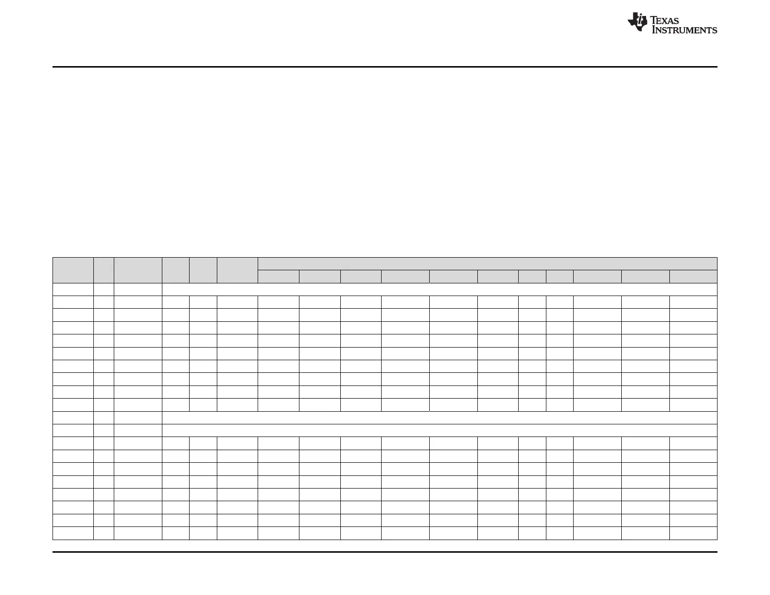
Table 2-1 provides a complete listing of the BoosterPack pins and the GPIO alternate functions available on each pin. The TM4C129ENCPDT
GPIO register GPIOPCTL values are shown for each configuration. The headers in this table are labeled from left to right in ten pin columns. ‘A’
and ‘D’ make up the outer BoosterPack standard pins, ‘B’ and ‘C’ make up the inner BoosterPack XL standard pins.
Table 2-1. BoosterPack 1 GPIO and Signal Muxing
Header Pin
Standard
Function GPIO
MCU
Pin Analog
Digital Function (GPIOPCTL Bit Encoding)
1 2 3 5 6 7 8 11 13 14 15
A1 1 +3.3 V 3.3 V
A1 2 Analog PE4 123 AIN9 U1RI - - - - - - - - - SSI1XDAT0
A1 3 UART RX PC4 25 C1- U7Rx - - - - - - - - - EPI0S7
A1 4 UART TX PC5 24 C1+ U7Tx - - - - RTCCLK - - - - EPI0S6
A1 5 GPIO PC6 23 C0+ U5Rx - - - - - - - - - EPI0S5
A1 6 Analog PE5 124 AIN8 - - - - - - - - - - SSIXDAT1
A1 7 SPI CLK PD3 4 AIN12 - I2C8SDA T1CCP1 - - - - - - - SSI2CLk
A1 8 GPIO PC7 22 C0- U5Tx - - - - - - - - - EPI0S4
A1 9 I2C SCL PB2 91 - - I2C0SCL T5CCP0 - - - - - - USB0STP EPI0S27
A1 10 I2C SDA PB3 92 - - I2C0SDA T5CCP1 - - - - - - USB0CLK EPI0S28
B1 1 +5 volts 5 V
B1 2 Ground GND
B1 3 Analog PE0 15 AIN3 U1RTS - - - - - - - - - -
B1 4 Analog PE1 14 AIN2 U1DSR - - - - - - - - - -
B1 5 Analog PE2 13 AIN1 U1DCD - - - - - - - - - -
B1 6 Analog PE3 12 AIN0 U1DTR - - - - - - - - - -
B1 7 Analog PD7 128 AIN4 U2CTS - T4CCP1 USB0PFLT - - NMI - - - SSI2XDAT2
B1 8 Analog PA6 40 - U2Rx I2C6SCL T3CCP0 USB0EPEN - - - - SSI0XDAT2 - EPI0S8
B1 9 A out PM4 74 TMPR3 U0CTS - T4CCP0 - - - - - - - -
B1 10 A out PM5 73 TMPR2 U0DCD - T4CCP1 - - - - - - - -