Functional Description
www.ti.com
14
SPMU372A–September 2015–Revised October 2016
Submit Documentation Feedback
Copyright © 2015–2016, Texas Instruments Incorporated
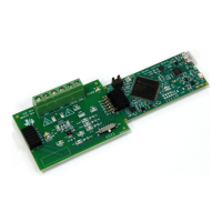
Hardware Description
2.1.7.2 BoosterPack 2
The second BoosterPack XL interface is located near the middle of the board. This interface is fully compliant with the BoosterPack standard and
adds features not covered by the BoosterPack standard that enable operation with additional BoosterPacks.
An additional analog signal is provided on the outer left header (X6-9). This signal can be used to monitor the touch panel on the popular Kentec
EB-LM4F120-L35 BoosterPack.
Using the jumpers JP4 and JP5, Controller Area Network (CAN) digital receive and transmit signals can be optionally routed to the BoosterPack 2
interface. The location of these signals is consistent with the CAN interface on the TM4C Series TM4C123G LaunchPad and the Stellaris
LM4F120 LaunchPad. In the default configuration, UART0 is used for the ICDI virtual UART and CAN is not present on the BoosterPack headers.
In this configuration, the ROM serial bootloader can be used over the ICDI virtual UART. When the jumpers are configured for CAN on the
BoosterPack, then UART2 must be used for the ICDI virtual UART.
To comply with both the original and the new BoosterPack standard, I2C is provided on both sides of the BoosterPack connection. Use of I2C on
the bottom left of the BoosterPack connection is highly encouraged where possible, to be in compliance with the new BoosterPack standard. To
provide I2C capability on the right side of the connector, per the original standard, two zero-ohm resistors (R19 and R20) are used to combine the
SPI and I2C signals. These signals are not shared with any other pins on the LaunchPad and therefore removal of these zero-ohm resistors
should not be required. Software should be certain that unused GPIO signals are configured as inputs.
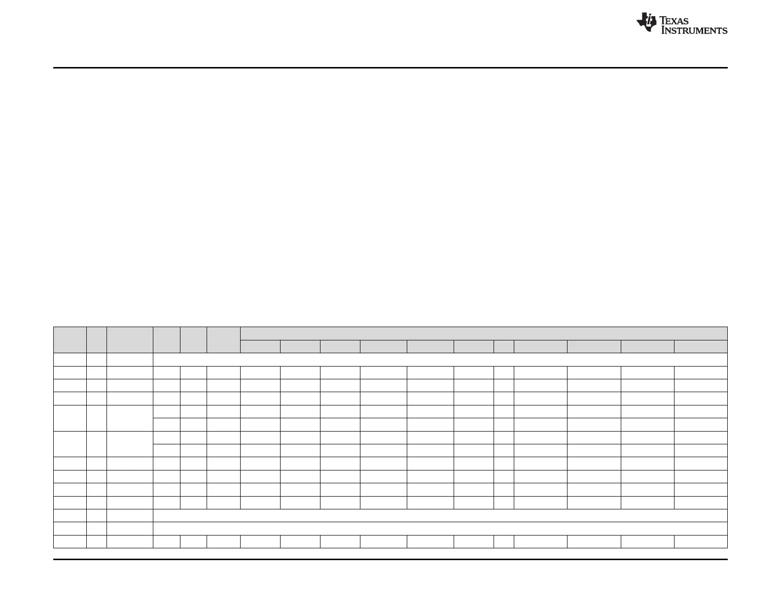
Table 2-2 provides a complete listing of the BoosterPack pins and the GPIO alternate functions available at each pin. The TM4C129ENCPDT
GPIO register GPIOPCTL values are shown for each configuration. The headers in this table are labeled from left to right in ten pin columns. ‘A’
and ‘D’ make up the outer BoosterPack standard pins, ‘B’ and ‘C’ make up the inner BoosterPack XL standard pins.
Table 2-2. BoosterPack 2 GPIO and Signal Muxing
Header Pin
Standard
Function GPIO
MCU
Pin Analog
Digital Function (FPIOPCTL Bit Encoding)
1 2 3 5 6 7 8 11 13 14 15
A2 1 3.3 V
A2 2 Analog PD2 3 AIN13 - I2C8SCL T1CCP0 C2o - - - - - - SSI2Fss
A2 3 UART RX PP0 118 C2+ U6Rx - - - - - - - - - SSI3XDAT2
A2 4 UART TX PP1 119 C2- U6Tx - - - - - - - - - SSI3XDAT3
A2 5
GPIO
(See JP4)
PD4 125 AIN7 U2Rx - T3CCP0 - - - - - - - SSI1XDAT2
PA0 33 - U0Rx I2C9SCL T0CCP0 - - CANORx - - - - -
A2 6
Analog
(See JP5)
PD5 126 AIN6 U2Tx - T3CCP1 - - - - - - - SSI1XDAT3
PA1 34 - U0Tx I2C9SDA T0CCP1 - - CAN0Tx - - - - -
A2 7 SPI CLK PQ0 5 - - - - - - - - - - SSI3Clk EPI0S20
A2 8 GPIO PP4 105 - U3RTS U0DSR - - - - - - - USB0D7 -
A2 9 I2C SCL PN5 112 - U1RI U3CTS I2C2SCL - - - - - - - EPIO0S35
A2 10 I2C SDA PN4 111 - U1DTR U3RTS I2C2SDA - - - - - - - EPIO0S34
B2 1 5 V
B2 2 GND
B2 3 Analog PB4 121 AIN10 U0CTS I2C5SCL - - - - - - - - SSI1Fss