USB-PD Modem
Digitally
Adjustable
VREF
Level
Shifter
Level
Shifter
Driver
Digitally
Adjustable
VREF
C_CC2
C_CC1
LDO_BMC
PD_TX
PD_RX
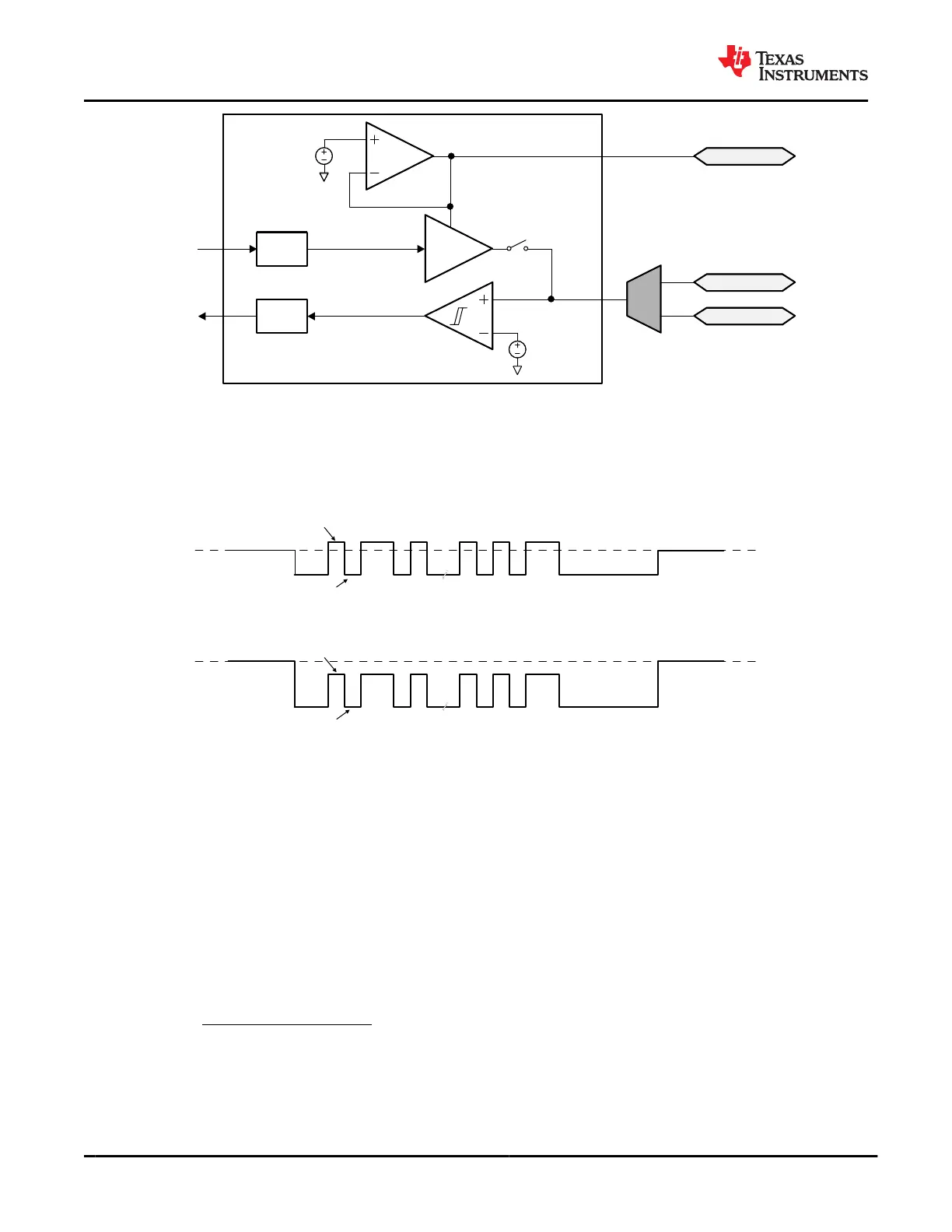
Figure 9-5. USB-PD BMC TX/Rx Block Diagram
Figure 9-6 shows the transmission of the BMC data on top of the DC bias. Note, The DC bias can be anywhere
between the minimum threshold for detecting a UFP attach (VD_CCH_USB) and the maximum threshold for
detecting a UFP attach to a DFP (VD_CCH_3P0) defined in the Cable Plugand Orientation Detection section.
This means that the DC bias can be below VOH of the transmitter driver or above VOH.
DC Bias DC Bias
VOH
VOL
DC Bias DC Bias
VOH
VOL
Figure 9-6. TX Driver Transmission with DC Bias
The transmitter drives a digital signal onto the C_CCn lines. The signal peak VTXP is adjustable by application
code and sets the VOH/VOL for the BMC data that is transmitted, and is defined in USB-PD TX Driver Voltage
Adjustment Parameter. Keep in mind that the settings in a final system must meet the TX masks defined in the
USB-PD Specifications.
When driving the line, the transmitter driver has an output impedance of ZDRIVER. ZDRIVER is determined by
the driver resistance and the shunt capacitance of the source and is frequency dependent. ZDRIVER impacts
the noise ingression in the cable.
Figure 9-7 shows the simplified circuit determining ZDRIVER. It is specified such that noise at the receiver is
bounded.
ZDRVER is defined by Equation 1.
R
DRIVER
DRIVER DRIVER
ZDRIVER
1 s R C
=
+ ´ ´
(1)
TPS65982
SLVSD02E – MARCH 2015 – REVISED AUGUST 2021
www.ti.com
36 Submit Document Feedback
Copyright © 2021 Texas Instruments Incorporated
Product Folder Links: TPS65982