Table 9-2. TPS65982 to USB Type-C Receptacle Mapping (continued)
DEVICE PIN Type-C RECEPTACLE PIN
C_SBU2 SBU2 (B8)
USB_RP_P/N
AUX_N
AUX_P
DEBUG3/4
DEBUG1/2
USB_EP_P/N
USB_EP_P/N
USB_RP_P/N
C_SBU2
C_SBU1
C_USB_BN
C_USB_BP
C_USB_TN
C_USB_TP
USB_RP_P
USB_RP_N
DEBUG2
DEBUG1
DEBUG4
DEBUG3
USB_RP
DEBUG3/4
DEBUG1/2
AUX_P/N
LSX_P2R
LSX_R2P
UART_TX
UART_RX
Digital Core
GPIO
Digital Cross-Bar Mux
UART0 UART1
UART0
CORE_
UART0
UART1
GPIO0
GPIO1
SWD
DEBUG3/4
DEBUG1/2
DEBUG3/4
DEBUG1/2
AUX_P/N
SWD_DATA
SWD_CLK
SWD_CLK/DATA
SWD_CLK/DATA
SWD_CLK/DATA
SBU_INT1
SBU_INT2
SBU_INT1
SBU_INT2
To ADC
Charger
ID
1st Stage 2nd Stage
UART1
CORE_
UART2
CORE_
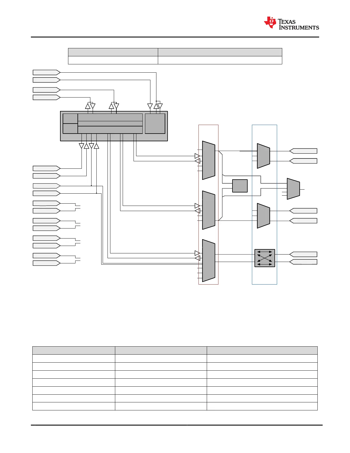
Figure 9-35. Port Data Multiplexers
Table 9-3 shows the typical signal types through the switch path. The UART_RX/TX and LSX_P2R/R2P paths
are digitally buffered to allow tri-state control for these paths. All other switches are analog pass switches. The
LSX_P2R/R2P pair is also configurable to be analog pass switches as well. These switch paths are not limited to
the specified signal type. For the signals that interface with the digital core, the maximum data rate is dictated by
the clock rate at which the core is running.
Table 9-3. Typical Signals through Analog Switch Path
INPUT PATH SIGNAL TYPE SIGNAL FUNCTION
SWD_DATA/CLK Single Ended Data, Clock
UART_RX/TX Single Ended TX/Rx UART
LSX_P2R/R2P Single Ended TX/Rx UART
DEBUG1/2/3/4 Single Ended Debug
AUX_P/N Differential DisplayPort and Thunderbolt AUX channel
USB_EP_P/N Differential USB 2.0 Low Speed Endpoint
USB_RP_P/N Differential USB 2.0 High Speed Data Root Port
TPS65982
SLVSD02E – MARCH 2015 – REVISED AUGUST 2021
www.ti.com
54 Submit Document Feedback
Copyright © 2021 Texas Instruments Incorporated
Product Folder Links: TPS65982