Time (50 Ps/div)
Current (A)
Voltage (V)
-0.5 -1
0 0
0.5 1
1 2
1.5 3
2 4
2.5 5
3 6
D011
I CC2
C_CC2
PP_CABLE
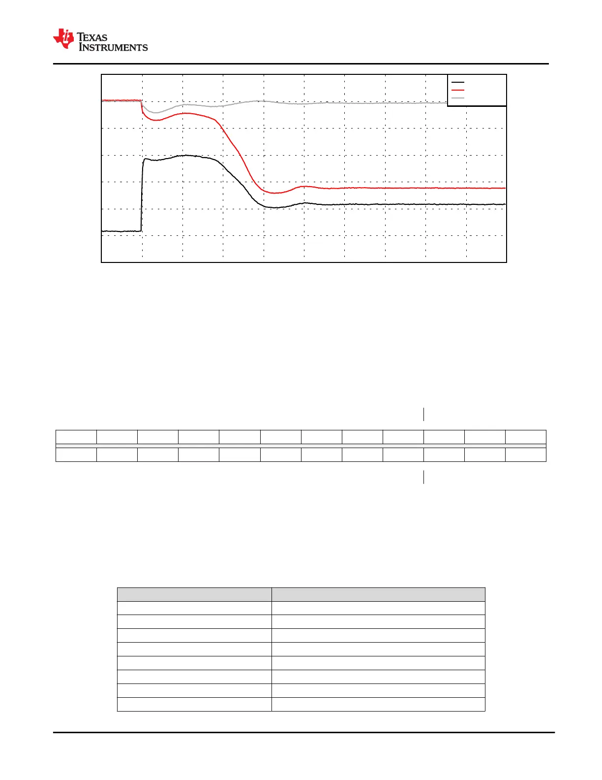
Figure 9-33. PP_CABLE to C_CCn Current Limit Response with a Soft Short (2 Ω)
9.3.4 USB Type-C Port Data Multiplexer
The USB Type-C receptacle pin configuration is show in Figure 9-34. Not all signals shown are required for all
platforms or devices. The basic functionality of the pins deliver USB 2.0 (D+ and D–) and USB 3.1 (TX and RX
pairs) data buses, USB power (VBUS) and ground (GND). Configuration Channel signals (CC1 and CC2), and
two Reserved for Future Use (SBU) signal pins. The data bus pins (Top and Bottom D+/D– and the SBU pins)
are available to be used in non-USB applications as an Alternate Mode (i.e., DisplayPort, Thunderbolt™, etc.).
Figure 9-34. USB Type-C Receptacle Pin Configuration
A1 A2 A3 A4 A5 A6 A7 A8 A9 A11 A11 A12
GND TX1+ TX1– VBUS CC1 D+ D– SBU1 VBUS RX2– RX2+ GND
GND RX1+ RX1– VBUS SBU2 D– D+ CC2 VBUS TX2– TX2+ GND
B12 B11 B10 B9 B8 B7 B6 B5 B4 B3 B2 B1
The TPS65982 USB Type-C interface multiplexers are shown in Table 9-2. The outputs are determined based
on detected cable orientation as well as the identified interface that is connected to the port. There are two USB
output ports that may or may not be passing USB data. When an Alternate Mode is connected, these same
ports may also pass that data (e.g. DisplayPort, Thunderbolt). Note, the TPS65982 pin to receptacle mapping is
shown in Table 9-2. The high-speed RX and TX pairs are not mapped through the TPS65982 as this would place
extra resistance and stubs on the high-speed lines and degrade signal performance.
Table 9-2. TPS65982 to USB Type-C Receptacle Mapping
DEVICE PIN Type-C RECEPTACLE PIN
VBUS VBUS (A4, A9, B4, B9)
C_CC1 CC1 (A5)
C_CC2 CC2 (B5)
C_USB_TP D+ (A6)
C_USB_TN D– (A7)
C_USB_BP D+ (B6)
C_USB_BN D– (B7)
C_SBU1 SBU1 (A8)
www.ti.com
TPS65982
SLVSD02E – MARCH 2015 – REVISED AUGUST 2021
Copyright © 2021 Texas Instruments Incorporated
Submit Document Feedback
53
Product Folder Links: TPS65982