comprised of the DEBUG_CTL1 and DEBUG_CTL2 pins. This third port is a firmware emulated I
2
C master. The
pins are generic GPIO and do not contain any dedicated hardware for I
2
C such as detecting starts, stops, acks,
or other protocol normally associated with I
2
C. This third port is always a master and has no interrupt. This
port is intended to master another device that has simple control based on mode and multiplexer orientation.
DEBUG_CTL1 is the serial clock and DEBUG_CTL2 is serial data.
The first two ports can be a master or a slave, but the default behavior is to be a slave. Port 1 and Port 2 are
interchangeable. Each port operates the same way and has the same access in and out of the core. An interrupt
mask is set for each that determines what events are interrupted on that given port.
9.5.2.1 I
2
C Interface Description
The TPS65982 support Standard and Fast mode I
2
C interface. The bidirectional I
2
C bus consists of the serial
clock (SCL) and serial data (SDA) lines. Both lines must be connected to a supply through a pullup resistor. Data
transfer may be initiated only when the bus is not busy.
A master sending a Start condition, a high-to-low transition on the SDA input/output, while the SCL input is high
initiates I
2
C communication. After the Start condition, the device address byte is sent, most significant bit (MSB)
first, including the data direction bit (R/W).
After receiving the valid address byte, this device responds with an acknowledge (ACK), a low on the SDA
input/output during the high of the ACK-related clock pulse. On the I
2
C bus, only one data bit is transferred
during each clock pulse. The data on the SDA line must remain stable during the high pulse of the clock period
as changes in the data line at this time are interpreted as control commands (Start or Stop). The master sends a
Stop condition, a low-to-high transition on the SDA input/output while the SCL input is high.
Any number of data bytes can be transferred from the transmitter to receiver between the Start and the Stop
conditions. Each byte of eight bits is followed by one ACK bit. The transmitter must release the SDA line before
the receiver can send an ACK bit. The device that acknowledges must pull down the SDA line during the ACK
clock pulse, so that the SDA line is stable low during the high pulse of the ACK-related clock period. When a
slave receiver is addressed, it must generate an ACK after each byte is received. Similarly, the master must
generate an ACK after each byte that it receives from the slave transmitter. Setup and hold times must be met to
ensure proper operation
A master receiver signals an end of data to the slave transmitter by not generating an acknowledge (NACK) after
the last byte has been clocked out of the slave. The master receiver holding the SDA line high does this. In this
event, the transmitter must release the data line to enable the master to generate a Stop condition.
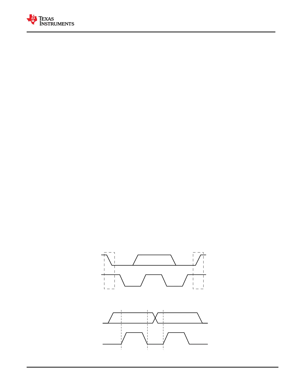
Figure 9-61 shows the start and stop conditions of the transfer. Figure 9-62 shows the SDA and SCL signals for
transferring a bit. Figure 9-63 shows a data transfer sequence with the ACK or NACK at the last clock pulse.
PS
Start Condition Stop Condition
SDA
SCL
Figure 9-61. I
2
C Definition of Start and Stop Conditions
Figure 9-62. I
2
C Bit Transfer
www.ti.com
TPS65982
SLVSD02E – MARCH 2015 – REVISED AUGUST 2021
Copyright © 2021 Texas Instruments Incorporated
Submit Document Feedback
77
Product Folder Links: TPS65982