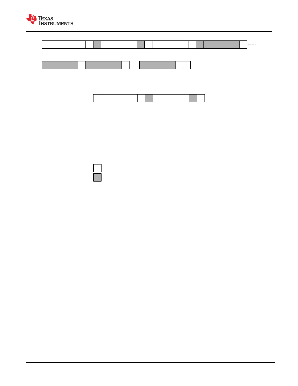
ASr Unique Address Rd Byte Count = NA
1 7 1 81 1
S Unique Address Wr Register NumberA
1 7 1 81 1
A
P
1
A
1
Data Byte N
81
AData Byte 1
8 1
AData Byte 2
8
Figure 9-65. I
2
C Unique Address Read Register Protocol
PS Slave Address Wr Data ByteA A
1 7 1 81 1
x x
1
S Start Condition
SR Repeated Start Condition
Rd Read (bit value of 1)
Wr Write (bit value of 0)
x Field is required to have the value x
A
Acknowledge (this bit position may be 0 for an ACK or
1 for a NACK)
P Stop Condition
Master-to-Slave
Slave-to-Master
Continuation of protocol
Figure 9-66. I
2
C Read/Write Protocol Key
9.5.2.5 I
2
C Pin Address Setting
To enable the setting of multiple I
2
C addresses using a single TPS65982 pin, a resistance is placed externally
on the I2C_ADDR pin. The internal ADC then decodes the address from this resistance value. Figure 9-67
shows the decoding. DEBUG_CTL1/2 are checked at the same time for the DC condition on this pin (high or
low) for setting other bits of the address described previously. Note, DEBUG_CTL1/2 are GPIO and the address
decoding is done by firmware in the digital core.
www.ti.com
TPS65982
SLVSD02E – MARCH 2015 – REVISED AUGUST 2021
Copyright © 2021 Texas Instruments Incorporated
Submit Document Feedback
79
Product Folder Links: TPS65982