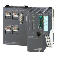
Manual BG41/BG42/BG43 Interface modules
Rev. 99/49 3-55
3.2.9.5.5 FB54 (UG/OG), establishing the upper and lower levels
With this data handling block FB54 (UG/OG) the lower and upper levels for one input/output or for
all inputs/outputs can be given. These values are used as a scaling.
The following parameters are to be transferred when loading FB54:
Des. Format Explanation
ADR KF Peripheral base address of the building
block
K/OU KY Number of the channels / analogue
outputs or inputs
UG KF Lower level for scaling
OG KF Upper level for scaling
FEHL BY Error byte
Tab. 3-12: List of parameters for the loading of the FB54
The following details are necessary for the abovementioned parameters:
ADR
(peripher)
Input of the peripheral address, under which the building block can be controlled
by the PLC. This address can be set with the DIL switches S1 and S2. Further
details can be found in chapter 5.
K/OU
K: Number of channels to which the module is connected (1-3).
OU: Number of analogue outputs or inputs (1-9)
At 9 the VALUE is set for all of the outputs or inputs of the module.
UG
Lower level, which is indicated at the smallest input/output value.
OG
Upper level, which is indicated at the highest input/output value.
FEHL
This byte has a value of 0, if functioning correctly. In the case of a malfunction an
error code is entered. The error is acknowledged automatically, i.e. the byte is
reset to 0 once the cause of the error has been eliminated.
1 Building block not ready
For a faultless functioning of the FB 54 it is required to set Bit 2 (lower limit
4mA) in FB51 under mode!

 Loading...