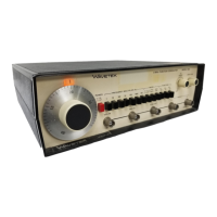
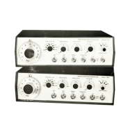
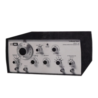
Model
2001
CIRCUIT DESCRIPTION
4.1
MECHANICAL ARRANGEMENT
Before beginning the actual circuit description, it would be
well to consider the mechanical arrangement of the instru-
ment. This will enable the following block diagram and cir-
cuit description to be associated with its physical position,
thereby, providing a better understanding of the overall in-
strument. The mechanical arrangement can be seen by re-
ferring to Figure 5-17 in the Maintenance section. This
TOP
VIEW
shows the Front Panel, plug-in module and the
rear chassis Power Supply sections.
4.2
SIMPLIFIED BLOCK DIAGRAM
The block diagram in Figure 4-1 contains both block and
module information. The blocks contained within each
module are indicated by the module outline.
The Power Supply provides three regulated voltage sources
of
+18, -18, and -20 volts for connections to the plug-in
modules.
The
M1H module generates the sweep ramp, blanking and
scope horizontal voltages.
The M2H module contains four distinct circuits; a -16 volt
reference supply,
a
+I6 volt reference supply, an inverted
sweep ramp supply, and the sweep drive circuits.
The two reference supplies and the two sweep ramp voltages
provide the signals to the
Frontpanel frequency and sweep
width controls. The signal from these controls is then fed
to the sweep drive circuit in the M2H module, where they
arecombined into a single signal, which drives the frequency
determined varactor diodes in the sweep oscillator modules.
Necessary level shifting, shaping and amplitude control is
provided by the sweep drive circuit.
The RF signal for BAND 1
(1
to 500 MHz) is generated in
the
M9H module where the signal from two sweep oscilla-
tors are combined in a diode mixer. The resultant,
difference signal, is fed to a
1-500 MHz pre-amplifier and
then to the MlOH module. This module contains a voltage
variable attenuator and the final 1-500 MHz amplifier.
The output from this amplifier is then fed to the
M19H
module where a PIN diode switch completes the circuit to
the RF output circuit.
error between the two voltages is amplified in the leveler
amplifier located in the MlOH module. The error voltage
is then connected to the voltage variable attenuator at the
input of the final 1 to 500 MHz amplifier. This closed loop
system maintains a constant amplitude
RF
signal at the
monitor point, which compensates for amplitude variation
in the sweep oscillator, mixer, and amplifier circuit and
also creates a zero impedance at the monitor point. In
order to create a 50 ohm source impedance, a 50 ohm
resistor is connected between the zero impedance point
and the RF output system.
The sweep oscillators for bands
2
&
3
are located in the
M19H module. The RF output from the oscillators is fed
through voltage variable attenuators directly to the RF
output circuit without amplification. Leveling for bands
2
&
3
is accomplished
in the same manner as for band 1.
The marker circuit is comprised of the marker adder
module
M5H, and the individual marker generators M6's.
In addition to the marker adding function of the M5H
module, it also provides for selection and leveling of the
sweep sample signal in the same manner as the main RF
output signal was leveled. This provides a constant ampli-
tude sweep sample signal to the individual marker modules
which is extremely important to obtain a "flat comb"
output from the harmonic generating marker modules.
It
also standardizes the sweep sample amplitude in all 2001
instruments, which insures proper operation of field in-
stalled markers.
This constant amplitude sweep sample signal is then fed to
the individual M6 marker modules where
it
is combined in a
mixer with a crystal controlled
CW
signal. The resultant
difference signals
(birdy markers) are then fed back
to the marker adder module where they are combined, am-
plified, and shaped into a single composite signal. This
signal is then fed through the marker size control and to
the Front Panel vertical output connector.
Leveling of the RF output is accomplished by a monitor
diode which measures the RF voltage and compares
it
to a
reference voltage supply by the vernier output control. Any
Model 2001
4.1
MECHANICAL
ARRANGEMENT
Before beginning the actual
circuit
description,
it
would
be
well
to
consider
the
mechanical arrangement
of
the
instru-
ment.
This
will
enable the
following
block
diagram and cir-
cuit
description
to
be associated
with
its physical
position,
thereby,
providing
a
better
understanding
of
the
overall
in-
strument.
The
mechanical arrangement can be
seen
by
re-
ferring
to
Figure 5-17 in the Maintenance section.
This
TOP
VIEW
shows
the
Front
Panel, plug-in
module
and the
rear chassis Power
Supply
sections.
4.2
SIMPLIFIED
BLOCK
DIAGRAM
The
block
diagram in Figure
4-1
contains
both
block
and
module
information.
The
blocks
contained
within
each
module
are indicated
by
the module
outline.
The
Power
Supply
provides three regulated voltage sources
of
+ 18, -18, and -20
volts
for
connections
to
the plug-in
modules.
The
M 1 H
module
generates
the
sweep
ramp,
blanking
and
scope
horizontal
voltages_
The
M2H
module
contains
four
distinct
circuits;
a -16
volt
reference
supply,
a
+16
volt
reference
supply,
an
inverted
sweep ramp
supply,
and the sweep
drive
circuits.
The
two
reference supplies and the
two
sweep
ramp
voltages
provide
the
signals
to
the
Front
Panel
frequency
and sweep
width
controls.
The
signal
from
these
controls
is
then fed
to
the sweep
drive
circuit
in
the
M2H
module,
where
they
are
combined
into
a single signal,
wh
ich drives the
frequency
determined
varactor
diodes
in
the
sweep
oscillator
modules.
Necessary level
shifting,
shaping and
amplitude
control
is
provided
by
the sweep
drive
circuit.
The RF signal
for
BAND
1
(1
to
500
MHz)
is
generated
in
the
M9H
module
where the signal
from
two
sweep oscilla-
tors
are
combined
in
a
diode
mixer.
The
resultant,
difference
signal,
is
fed to a 1-500
MHz
pre-amplifier
and
then
to
the
Ml0H
module.
This
module
contains
a voltage
variable
attenuator
and the
final
1-500
MHz
amplifier.
The
output
from
this
amplifier
is
then fed
to
the
M19H
module
where a PIN
diode
switch
completes
the
circuit
to
the
RF
output
circuit.
Leveling
of
the
RF
output
is
accomplished
by
a
monitor
diode
which
measures
the
RF
voltage and compares
it
to
a
reference voltage
supply
by
the
vernier
output
control.
Any
CIRCUIT
DESCRIPTION
error
between the
two
voltages
is
amplified
in the leveler
amplifier
located in the M 1
OH
module.
The
error
voltage
is
then
connected
to
the voltage variable
attenuator
at
the
input
of
the
final
1
to
500
MHz
amplifier.
This
closed
loop
system
maintains
a
constant
amplitude
RF
signal at the
monitor
point,
which
compensates
for
amplitude
variation
in the sweep
oscillator,
mixer,
and
amplifier
circuit
and
also creates a zero impedance at the
monitor
point.
In
order
to
create a
50
ohm
source impedance, a
50
ohm
resistor
is
connected between the zero impedance
point
and the R F
output
system.
The sweep oscillators
for
bands 2 & 3 are located in the
M19H
module.
The
RF
output
from
the oscillators
is
fed
through
voltage variable
attenuators
directly
to
the RF
output
circuit
without
amplification.
Leveling
for
bands
2
& 3
is
accomplished
in
the
same
manner
as
for
band
1.
The
marker
circuit
is comprised
of
the
marker
adder
module
M5H,
and the
individual
marker
generators M6's.
In
addition
to
the
marker
adding
function
of
the
M5H
module,
it
also provides
for
selection and leveling
of
the
sweep sample signal in the same
manner
as
the
main
RF
output
signal was leveled.
This
provides a
constant
ampli-
tude
sweep sample signal
to
the
individual
marker
modules
which
is
extremely
important
to
obtain
a
"flat
comb"
output
from
the
harmonic
generating
marker
modules.
It
also standardizes the sweep sample
amplitude
in
all 2001
instruments,
which
insures
proper
operation
of
field
in-
stalled markers.
Th
is
constant
amplitude
sweep sample signal is then fed
to
the
individual
M6
marker
modules
where
it
is
combined
in
a
mixer
with
a crystal
controlled
CW
signal.
The
resultant
difference
signals
(birdy
markers)
are
then
fed
back
to
the
marker
adder
module
where
they
are
combined,
am-
plified,
and shaped
into
a single
composite
signal.
This
signal
is
then fed
through
the
marker
size
control
and
to
the
Front
Panel vertical
output
connector.
4-3
 Loading...