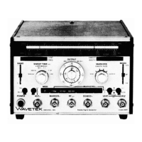
Model
2001
CIRCUIT DESCRIPTION
positive, full output is retained (a diode opens the vernier
ground connection) producing a nearly constant retrace
time.
For triggered modes, the negative threshold of the hysteresis
switch is shifted out of the way by a diode and resistor con-
nected through 014 or through
S102D, when in "line''
position. The integrator will now continue its negative ramp
until
it
is
stopped by a clamp circuit turned on by a com-
parator. The integrator output
is
now held at this level
un-
less a trigger is applied to the hysteresisswitch. A trigger
cannot flip
the hysteresis switch until this clamp level is
reached because the triggers must pass through an amplifier
which is gated off until the clamp comparator
(09) con-
ducts.
Triggers are prevented from reaching the hysteresis switch
(pin 6) by a voltage at pin 1, which causes comparator
08
to open FET switch 014. The primary function of the vol-
tage at pin 1 is to shift the clamp comparator input out of
the way to allow free-running oscillations.
Since the integrator is an inverting amplifier, and both input
(pin
7)
and output (pin 8) are available, a feedback resistor
network allows the SWEEP TlME vernier, R 102, to be used
as a dc level shifter in the manual
mode. A non-inverting
amplifier consisting of Q6,
07 and Q19, with a gain of
2,
provide a 32 volt peak-to-peak wave output which is used for
sweep drive. This output is divided by R 18 and R53 to pro-
vide a horizontal drive of about 16 volts peak-to-peak at an
impedance of about 23K ohms.
A centering adjustment (R4
1)
provides a dc level adjustment
of the integrator and horizontal outputs (pin 8, pin
12,
and
pin 11) by shifting both positive and negative thresholds of
the hysteresis switch. A size adjustment
(R45) provides an
amplitude adjustment by effectively varying the size of the
hysteresis window. Symmetry of trace and retrace time
(for equal positive and negative input voltages to the inte-
grator) is established by adjusting the integrator balance
control R7. This adjustment also affects the manual mode
centering and the sweep period for fully counterclockwise
rotation of the SWEEP TlME vernier.
The four sections of the SWEEP TlME selector switch pro-
gram the
MlH module. The functions of each section are
listed below
:
Section A Integrator input selector
Section B Clamp level shift and routing switch
disconnect
Section
C
Trigger source selector
Section D Line trigger routing, and hysteresis
switch hold.
Circuit operation as modified by the switch positions may
be understood by considering the MANUAL, VARIABLE
RATE, and LINE positions one at a time.
MANUAL POSITION
Section A. A feedback resistor
R 113 is connected from
output (pin 8) to input (pin 7) of the integrating amplifier,
converting
it
to an inverting dc amplifier. Resistor R 114
shifts the amplifier output dc level to -8 volts for zero input
voltage to
R104. When the SWEEP TlME vernier control
R102
is
fully clockwise, the negative input voltage to R 104
is sufficient to shift the output voltage to
+8 volts dc.
Section B. The clamp is disabled in this position by apply-
ing
+18V to pin
I,
causing the hysteresis switch input to be
disconnected from any internal source of triggers by open-
ing the routing switch 014 (since
Q8 is turned off). The
shift bias is disconnected when 014 is open.
Section C. The trigger input point pin
4
is
grounded.
Section D.
The hysteresis switch is held in one state by
applying -18 volts to its input through a 33K ohm resistor.
This causes the output to be negative (this bistable circuit is
a positive feedback amplifier) providing the proper polarity
to R102 and preventing blanking of the RF output.
VARIABLE RATE POSITIONS
Section A. Proper integrator input resistors are selected in
decade increments in these positions, R 105
-
R 108.
Section B. The clamp is disabled and triggers are held off
unless the "pull trigger" switch is opened, removing
+I8
volts.
Section C. Two trigger sources are connected to pin 4; an
external trigger from REMOTE jack
J101-7 and triggers
from the Front Panel momentary
TRIG switch S103.
Section D. No connection is made to pin
6
in any of the
four variable rate positions.
LINE POSITION
Section A. The proper value integrating resistor
is
selected,
by-passing the SWEEP TlME vernier, to produce equal
sweep and retrace periods.
Section B. Clamping, works in this position independently
of the "pull trig" switch.
Section
C.
The line rate square
wave
from the power supply
is connected to the trigger input.
Model 2001
positive,
full
output
is
retained
(a
diode
opens
the
vernier
ground
connection)
producing
a nearly
constant
retrace
time.
For
triggered modes, the negative
threshold
of
the
hysteresis
switch
is
shifted
out
of
the
way
by
a
diode
and resistor con-
nected
through
014
or
through
S102D,
when
in
"line"
position.
The
integrator
will
now
continue
its
negative ramp
until
it
is stopped
by
a cfamp circu
it
turned
on
by
a com-
parator.
The
integrator
output
is
now
held
at
this
level un-
less
a trigger is applied
to
the
hysteresis
switch.
A trigger
cannot
flip
the hysteresis
switch
until
this
clamp
level
is
reached because
the
triggers
must
pass
through
an
amplifier
which
is gated
off
until
the
cfamp
comparator
(09)
con-
ducts.
Triggers are prevented
from
reaching the hysteresis
switch
(pin
6)
by
a voltage at
pin
1,
which
causes
comparator
08
to
open
FET
switch
014.
The
primary
function
of
the
vol-
tage
at
pin
1
is
to
shift
the
clamp
comparator
input
out
of
the
way
to
allow
free-running
oscillations.
Since
the
integrator
is
an
inverting
amplifier,
and
both
input
(pin
7) and
output
(pin
8) are available, a feedback resistor
network
allows
the
SWEEP
TIME
vernier, R 102,
to
be used
as
a
dc
level
shifter
in the manual mode. A
non-inverting
amplifier
consisting
of
06,07
and
019,
with
a gain
of
2,
provide
a 32
volt
peak-to-peak wave
output
which
is used
for
sweep drive.
This
output
is
divided
by
R
18
and
R53
to
pro-
vide a
horizontal
drive
of
about
16
volts
peak-to-peak at
an
impedance
of
~bout
23K
ohms.
A
centering
adjustment
(R41)
provides a
dc
level
adjustment
of
the
integrator
and
horizontal
outputs
(pin
8,
pin
12, and
pin
11)
by
shifting
both
positive and negative
thresholds
of
the
hysteresis
switch.
A size
adjustment
(R45)
provides
an
amplitude
adjustment
by
effectively
varying
the
size
of
the
hysteresis
window.
Symmetry
of
trace and retrace
time
(for
equal
positive
and negative
input
voltages
to
the inte-
grator) is established
by
adjusting the
integrator
balance
control
R7.
This
adjustment
also
affects
the manual mode
centering
and
the sweep
period
for
fully
counterclockwise
rotation
of
the SWEEP
TIME
vernier.
The
four
sections
of
the
SWEEP
TIME
selector
switch
pro-
gram
the
M 1 H
module.
The
functions
of
each section are
listed
below:
Section
A
Section
B
Section C
Section
D
I
ntegrator
input
selector
Clamp
level
shift
and
routing
switch
disconnect
Trigger source selector
Line
trigger
routing,
and hysteresis
switch
hold.
CIRCUIT
DESCRIPTION
Circuit
operation
as
modified
by
the
switch
positions
may
be
understood
by
considering the
MANUAL,
VARIABLE
RATE,
and
LINE
positions
one
at
a
time.
MANUAL
POSITION
Section
A.
A feedback resistor R 113 is connected
from
output
(pin
8)
to
input
(pin
7)
of
the
integrating
amplifier,
converting
it
to
an
inverting
dc
amplifier.
Resistor R 114
shifts
the
amplifier
output
dc
level
to
-8
volts
for
zero
input
voltage
to
R 104. When
the
SWEEP
TIME
vernier
control
R 1 02
is
fu
lIy
clockwise, the negative
input
voltage
to
R 104
is
sufficient
to
shift
the
output
voltage
to
+8
volts
dc.
Section
B.
The
clamp
is
disabled
in
this
position
by
apply-
ing +
18V
to
pin
1, causing the hysteresis
switch
input
to
be
disconnected
from
any
internal
source
of
triggers
by
open-
ing the
routing
switch
014
(since
08
is
turned
off).
The
shift
bias
is
disconnected
when
014
is open.
Section
C.
The
trigger
input
point
pin
4 is grounded.
Section
D. The hysteresis
switch
is
held in one state
by
applying
-18
volts
to
its
input
through
a
33K
ohm
resistor.
This
causes the
output
to
be negative
(this
bistable
circuit
is
a
positive
feedback
amplifier)
providing
the
proper
polarity
to
R 1 02 and
preventing
blanking
of
the
R F
output.
VARIABLE
RATE
POSITIONS
Section
A.
Proper
integrator
input
resistors are selected in
decade
increments
in these
positions,
R
105
- R 1 08.
Section
B.
The
clamp
is
disabled and triggers are held
off
unless
the
"pull
trigger"
switch
is
opened,
removing
+18
volts.
Section
C.
Two
trigger sources are
connected
to
pin
4;
an
external trigger
from
REMOTE
jack
J 101-7 and triggers
from
the
Front
Panel
momentary
TRIG
switch
S103.
Section
D.
No
connection
is
made
to
pin
6 in any
of
the
four
variable rate positions.
LINE
POSITION
Section
A.
The
proper
value
integrating
resistor
is
selected,
by-passing the SWEEP
TIME
vernier,
to
produce
equal
sweep and retrace periods.
Section
B.
Clamping,
works
in
this
position
independently
of
the
"pull
trig"
switch.
Section
C.
The line rate square wave
from
the power supply
is
connected
to
the
trigger
input.
4-5
 Loading...