KC705 Getting Started Guide www.xilinx.com 17
UG883 (v4.0.1) May 28, 2014
AMS Bring-up with the AMS101 Evaluation Card
Evaluating AMS
1. Connect and power the hardware:
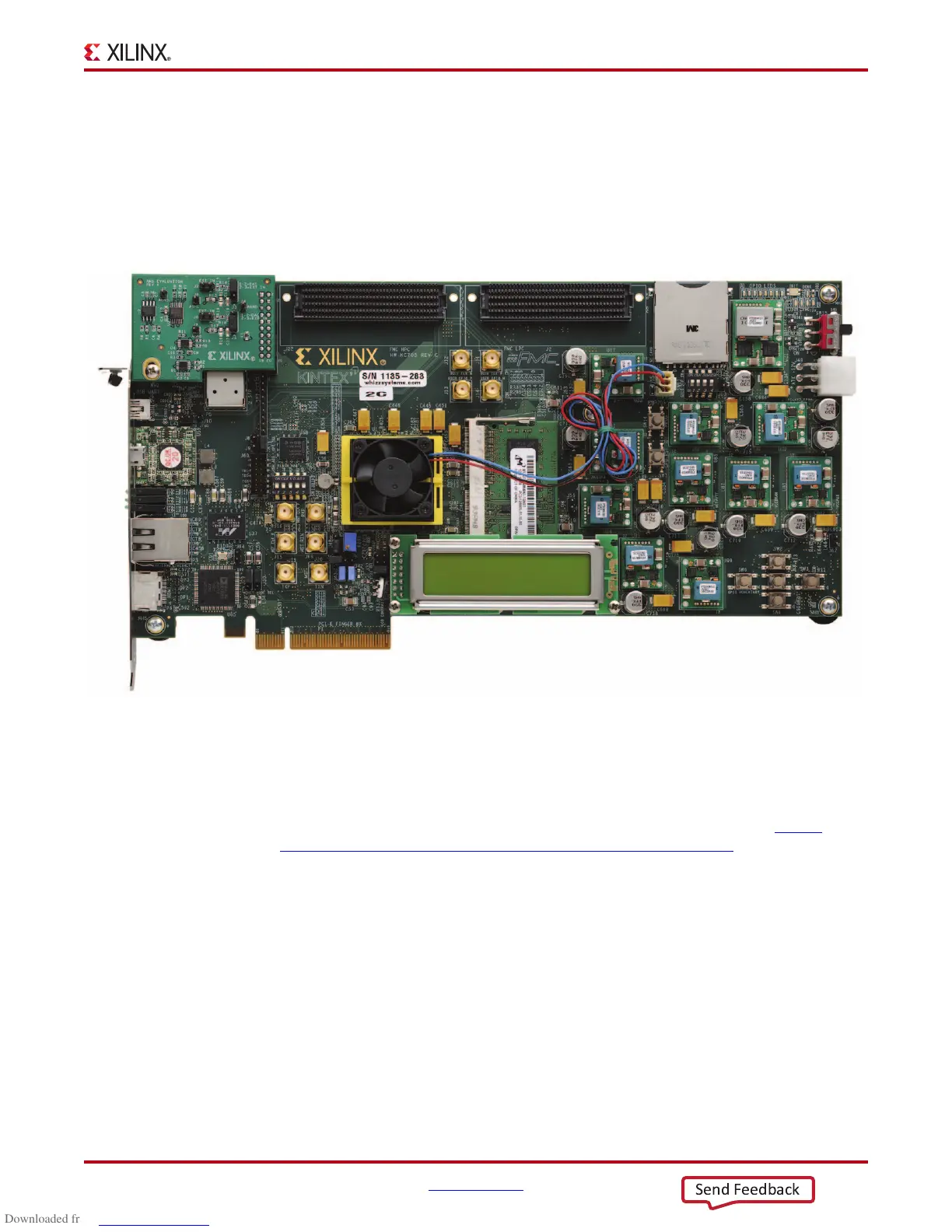
a. Plug the AMS101 evaluation card into the XADC header on your FPGA base
board.
Note:
Ensure the notch on the XADC header lines up correctly with the AMS101
evaluation card (see Figure 8).
b. Power up the FPGA base board
2. Download the design to the FPGA. Installation of ISE Programming tools or Lab Tools
is required for downloading the bitstream to the FPGA.
Refer to the Vivado Design Suite User Guide: Programming and Debugging (UG908
) at
http://www.xilinx.com/support/documentation/dt_vivado.htm
to obtain
information on downloading the design to the FPGA.
a. Open the xadc_eval_design.bit file from the AMS Targeted Reference
Design files.
3. Run the AMS101 Evaluator LabVIEW GUI executable from your desktop. After
loading the AMS Evaluator installer files, a red X with the AMS Evaluator program
should reside on your desktop.
Note:
The AMS bitstream can also be loaded with ChipScope analyzer.
X-Ref Target - Figure 8
Figure 8: KC705 Base Board with AMS101 Evaluation Card Plugged into XADC Header

 Loading...


