KC705 Getting Started Guide www.xilinx.com 19
UG883 (v4.0.1) May 28, 2014
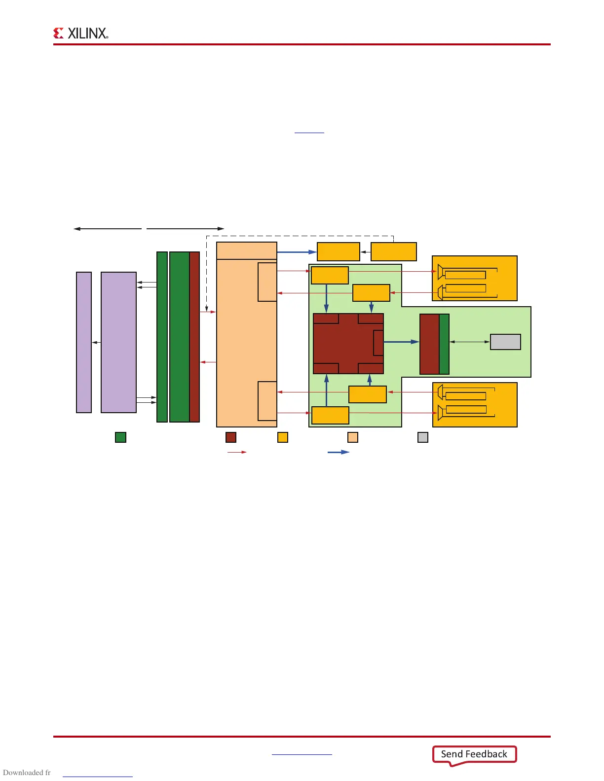
Advanced Bring-up Using the Base Targeted Reference Design
Advanced Bring-up Using the Base Targeted Reference Design
The primary components of the Kintex-7 FPGA Base TRD are:
• Integrated Endpoint block for PCI Express (PCIe). See 7 Series FPGAs Integrated Block
for PCI Express User Guide (UG477
).
• Northwest Logic Packet DMA [Ref 5]
• Multiport Virtual FIFO
The TRD system can sustain up to 10 Gb/s throughput end to end.
Figure 10 provides an overview of the TRD.
Note:
In Figure 10 the arrows indicate AXI interface directions (from master to slave). They do not
indicate data flow directions.
X-Ref Target - Figure 10
Figure 10: Kintex-7 FPGA Base TRD Block Diagram
UG883_10_121112
Multiport Virtual FIFO
DDR3 I/O
Software
Multi-Channel
DMA for PCIe
DDR3
Channel-0
C2SS2C
Channel-1
S2C C2S
64 x
1,600 Mb/s
PCIe x4Gen2 Link / PCIe x8Gen1 Link
VFIFO
Controller
Software
Driver
Interface Blocks in FPGA
Third Party IPXilinx IP On BoardCustom Logic
AXI-ST AXI-MM
Hardware
VFIFO
Controller
VFIFO
Controller
VFIFO
Controller
Raw Packet Data Block
Checker
Generator
L
oopback
Loopback
Raw Packet Data Block
Generator
Checker
User Space
Registers
Target Interface
AXI Master
256 x
200 MHz
64 x 250 MHz
64 x
250 MHz
64 x
250 MHz
64 x
250 MHz
64 x
250 MHz
Performance
Monitor
GUI
GTX Transceiver
Integrated Endpoint Block for PCI Express
AXI-ST Basic Wrapper
AXI
MIG
AXI
Interconnect
SI
SI
SI SI
MI

 Loading...


