22 www.xilinx.com KC705 Getting Started Guide
UG883 (v4.0.1) May 28, 2014
Advanced Bring-up Using the Base Targeted Reference Design
Board Setup
This section describes how to set up the KC705 Evaluation board required to demonstrate
the TRD.
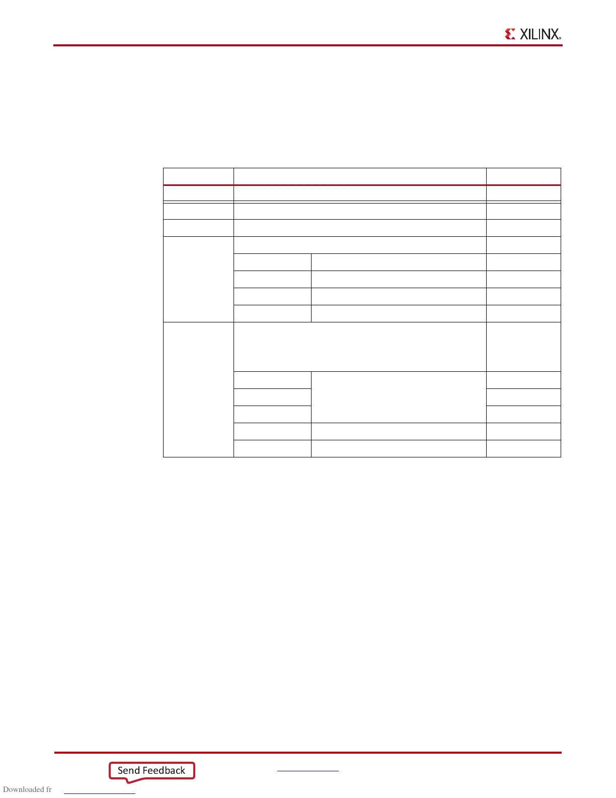
1. Set the KC705 Jumpers and Switches: Verify that the KC705 Evaluation board jumpers
and switches are set as shown in Table 3 and Figure 11.
Tab le 3 : Switch and Jumper Settings
Jumper Function Setting
J32 PCIe configuration width — 4 lane design Jump 3-4
Switch Function or Type Setting
SW15 Board power slide-switch Off
SW11 User GPIO DIP switch
4 Off
3 Off
2 Off
1 Off
S13 DIP switch SW13 positions 1 and 2 control the setting of address bits
of the flash.
DIP switch SW13 positions 3, 4, and 5 control which configuration
mode.
5 (M0) M2 =0 M1=1 M0=0 – Master BPI
M2 =0 M1=0 M0=1 – Master SPI
M2 =1 M1=0 M0=1 – JTAG
Off
4 (M1) On
3 (M2) Off
2 Off
1 Off

 Loading...


