KC705 Getting Started Guide www.xilinx.com 23
UG883 (v4.0.1) May 28, 2014
Advanced Bring-up Using the Base Targeted Reference Design
Hardware Bring-Up
This section presents steps for hardware bring-up.
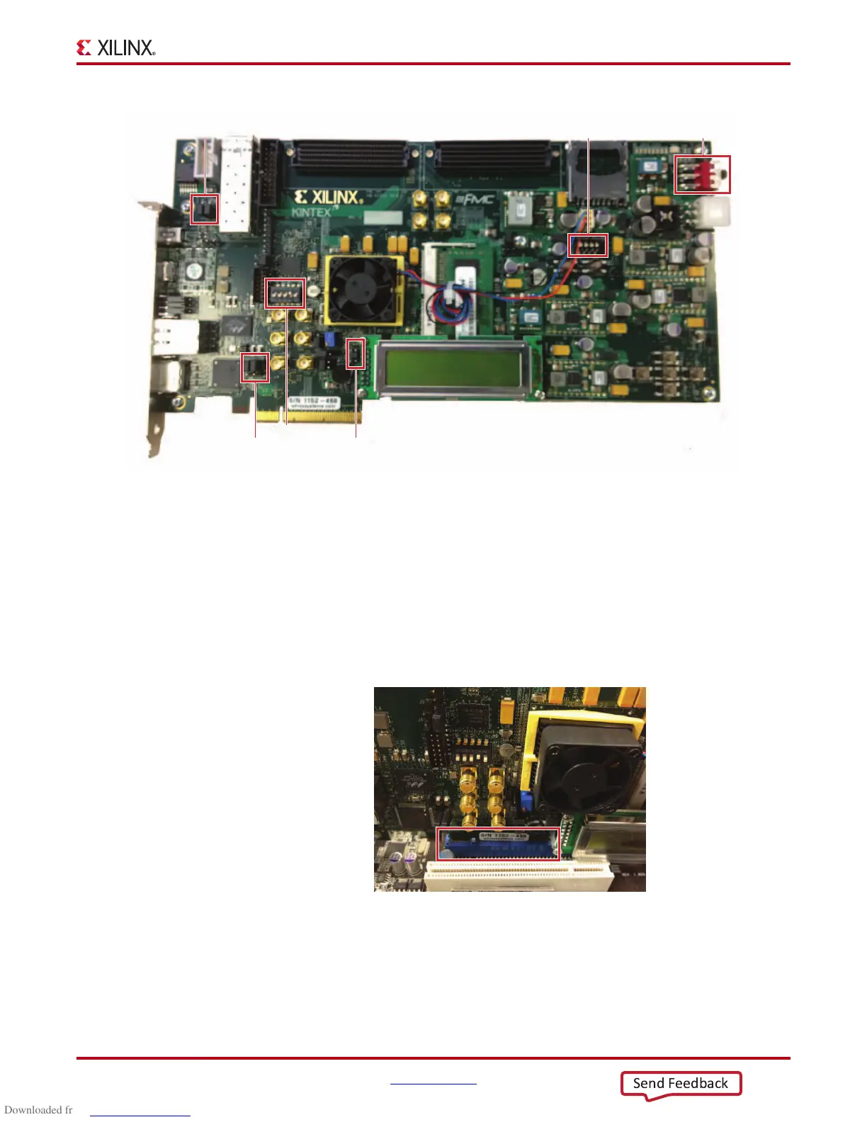
1. With the host system switched off, insert the KC705 board in the PCIe slot through the
PCI Express x8 or x16 edge connector (Figure 12).
The TRD programmed on the KC705 board has a 4-lane PCIe v2.0 configuration,
running at a 5 Gb/s link rate per lane. The PCI Express specification allows for a
smaller lane width Endpoint to be installed into a larger lane width PCIe connector.
X-Ref Target - Figure 11
Figure 11: Switch and Jumper Settings
UG883_11_040913
J27, J28
J29, J30
SW13
J32
SW15SW11
X-Ref Target - Figure 12if
Figure 12: KC705 Board Plugged into a PCIe x16 Slot

 Loading...


