KC705 Getting Started Guide www.xilinx.com 25
UG883 (v4.0.1) May 28, 2014
Advanced Bring-up Using the Base Targeted Reference Design
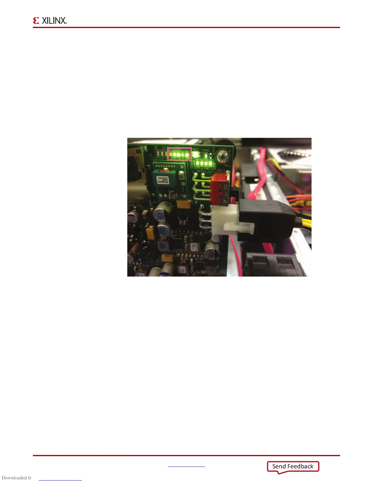
4. Verify the status of the design on the KC705 LEDs. The design provides status on the
GPIO LEDs on the upper right of the KC705 board (Figure 14). After the PC system is
powered on and the TRD has successfully configured, status LEDs, from right to left,
should indicate:
• LED 0 — ON if the PCIe link is up
• LED 1 — Flashes if the PCIe user clock is present
• LED 2 — ON if lane width is what is expected, else it flashes (for a 4 lane design, the
expected lane width is 4; for an 8 lane design, the expected lane width is 8)
• LED 3 — ON if memory calibration is done
• LED 4 to LED 7 — Not connected
X-Ref Target - Figure 14
Figure 14: Location of GPIO Status LEDs (Indicates TRD Status)

 Loading...


