KC705 Getting Started Guide www.xilinx.com 27
UG883 (v4.0.1) May 28, 2014
Advanced Bring-up Using the Base Targeted Reference Design
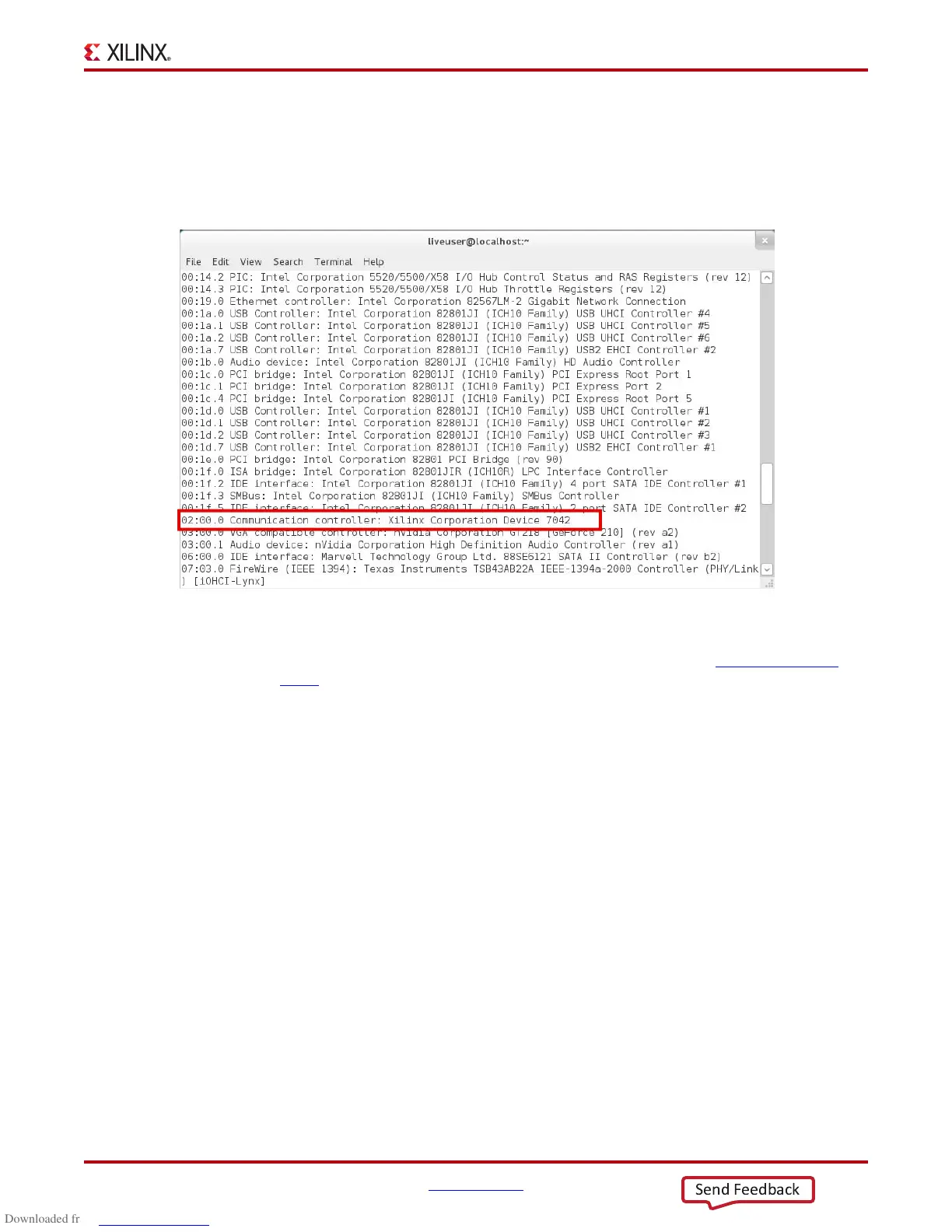
This message confirms that the design programmed into the KC705 board has been
found by the BIOS and the Fedora 16 OS. The bus number varies depending on which
PC motherboard and slot are used. Figure 16 shows a lspci output for an example
system. Xilinx device 7042 has been found by the BIOS on bus number 2 (02:00.0 -
bus:dev.function).
4. Download the reference design from the Docs & Designs tab at www.xilinx.com/
kc705 and copy the k7_pcie_dma_ddr3_base folder into any directory.
5. To set up and run the TRD demonstration, the software driver should be installed on
the PC system. Software driver installation involves:
a. Building the kernel objects and the GUI
b. Inserting the driver modules into the kernel.
After the driver modules are loaded, the application GUI can be invoked. The user can
set parameters through the GUI and run the TRD.
When the user is done running the TRD, the application GUI can be closed and the
drivers can be removed.
A script is provided to execute all the above actions so that the user can quickly start
the TRD.
The k7_trd_lin_quickstart script is available in the k7_pcie_dma_ddr3_base
folder. Right click the script, select properties, go to the permissions tab, check
the box Allow executing file as program—this makes the script executable.
Close the window.
X-Ref Target - Figure 16
Figure 16: PCI and PCI Express Bus Devices
UG883_16_040913

 Loading...


