EasyManuals Logo

Xilinx Kintex-7 FPGA KC705 User Manual

Xilinx Kintex-7 FPGA KC705
40 pages
To Next Page IconTo Next Page
To Previous Page IconTo Previous Page
Page #31 background imageLoading...
Page #31 background image
KC705 Getting Started Guide www.xilinx.com 31
UG883 (v4.0.1) May 28, 2014
Advanced Bring-up Using the Base Targeted Reference Design
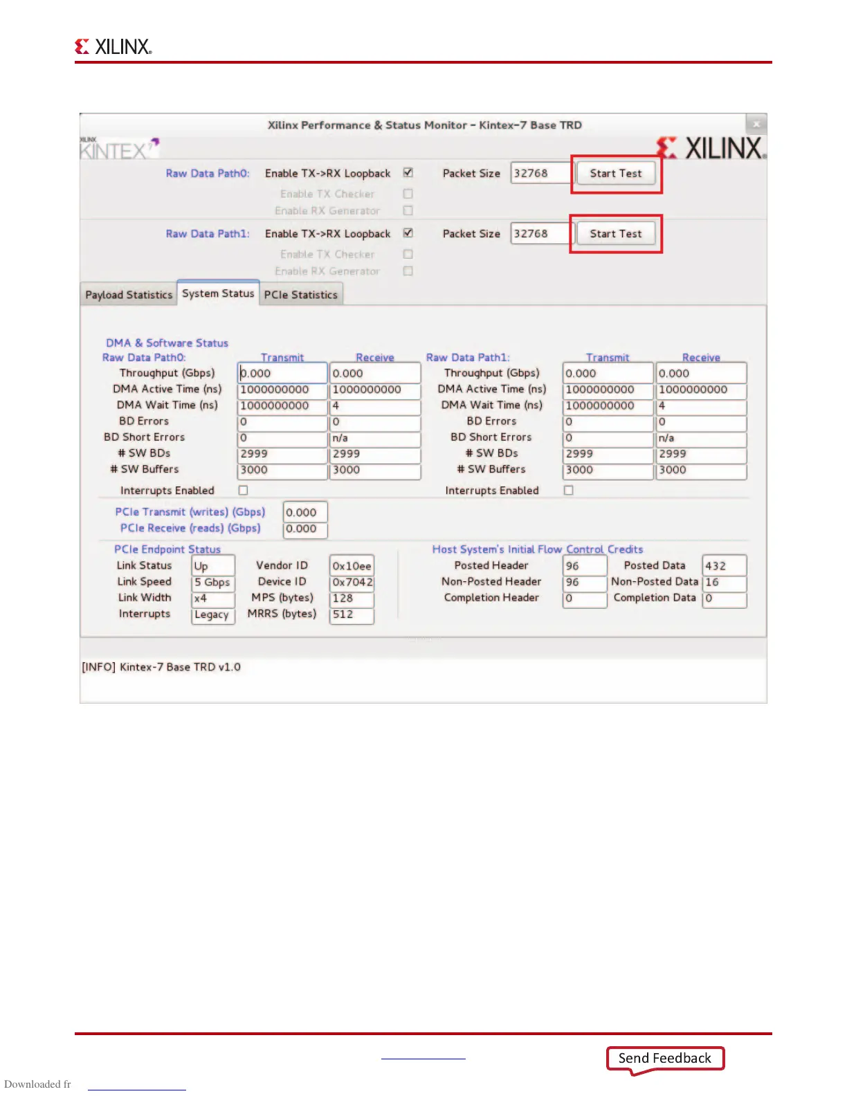
3. Verify TRD operations through the status information provided by the GUI (see
Figure 21).
a. Verify the PCIe throughput.
b. Verify the DMA channel throughput for the Raw Data Path0.
c. Verify the DMA channel throughput for the Raw Data Path1.
d. Verify there are no buffer descriptor errors for error-free operation.
X-Ref Target - Figure 20
Figure 20: Start Data Traffic from the Performance Monitor
UG883_20_121112
Send Feedback

Other manuals for Xilinx Kintex-7 FPGA KC705

Questions and Answers:

Question and Answer IconNeed help?

Do you have a question about the Xilinx Kintex-7 FPGA KC705 and is the answer not in the manual?

Xilinx Kintex-7 FPGA KC705 Specifications

General IconGeneral
FPGA Speed Grade-2
FPGA PackageFFG900
Logic Cells326, 080
DSP Slices840
Clock Management Tiles10
Transceivers16
DDR3 Memory1GB
Flash Memory128MB
Clock200 MHz oscillator
Form FactorATX
Ethernet10/100/1000
Expansion ConnectorsFMC
USBUSB-UART

Related product manuals