30 www.xilinx.com KC705 Getting Started Guide
UG883 (v4.0.1) May 28, 2014
Advanced Bring-up Using the Base Targeted Reference Design
2. To start data traffic on the two data paths:
a. Click Start Test on Raw Data Path0 as shown in Figure 20. This enables the
driver to start generating the data for Raw Data Path0.
b. Click Start Test on Raw Data Path1 as shown in Figure 20. This enables the
driver to start generating the data for Raw Data Path1.
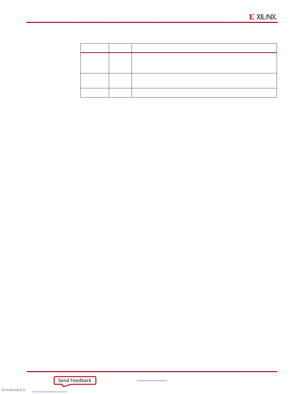
Tab le 4 : KC705 Board Status Field Explanations
Field Status Explanation
Link Status Up This confirms that the PCIe link is up and a PCIe connection is
established between the Kintex-7
FPGA Endpoint for PCI Express
and the PC motherboard chipset.
Link Speed 5.0 Gb/s This confirms that the PCIe link is operating at line rate speed per
PCI Express, v2.0.
Link Width x4 This confirms that the PCIe link is trained as a x4 link.

 Loading...


