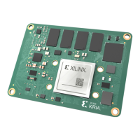
The K26 SOM 3D CAD les are available for your plaorm or carrier design reference. These
les are design aides in your cooling mechanical design, system assembly interference and
clearance reviews, and board-to-board (B2B) connector placement alignment checks.
PCB Fabrication and Assembly House
Requirements
The following are requirements for the fabricaon of the PC board assembly.
• Carrier card PCB pad-to-pad tolerance should be < ±25 µm.
The blue to red cross (surface pad to surface pad) tolerance with respect to the Gerber pad
locaon should be less than ±1mil (25 µm).
• Carrier card assembly house placement capability should be < ±26 µm.
• RMS value of the PCB pad-to-pad and component placement tolerance, based on the
capabilies listed above should be < ±36 µm.
• Samtec recommends a tolerance of ±0.04 mm in the distance between the connectors.
• The combinaon of the all these requirements must be controlled to less than ±40 µm
The evaluaon of Samtec connector placement is conducted by shiing the placement of the
connector from 0% (PCB pad center aligned with connector pin center) to 15% (pin center oset
by 15% of PCB pad width). The shied connectors are capable of self-aligning aer a reow
soldering process. The following image shows that even though placement of the connector
shied by 15% of the pad width, the connector solder ball was sll able to self-align to the center
of pad.
Chapter 3: Mechanical Design Considerations
UG1091 (v1.0) April 20, 2021 www.xilinx.com
Carrier Card Design for Kria SOM 39

 Loading...