Note: PCB fab and assembly contractors must be able to produce carrier cards to the specicaons listed
in the PCB Fabricaon and Assembly House Requirements secon. In addion, the connectors that are
shied by 15% of the pad width must be capable of self-aligning aer a reow soldering process.
SOM to Carrier Card Samtec Connector
Placement Guidelines
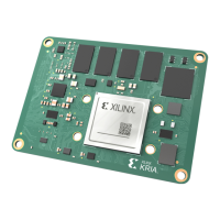
Both the commercial (C) grade and industrial (I) grade SOMs have two Samtec 0.635 mm
AcceleRate
®
HD high-density, 4-row, 60-posion connectors. The Samtec part number is ADF6–
60–03.5–L–4–2–A. The connectors are placed on the boom side of the carrier card centered
between the mounng holes shown in Figure 2: K26 SOM Dimensions.
Board-to-board (B2B) mang connectors must be precisely placed on the PCB, parcularly for
mul-pair connector applicaons. Tight control is required during the board layout design and
the manufacturing process for product reliability and a decent yield rate. To avoid over-stressing
the mechanical design of the connectors and creang funconal damage during system assembly,
the next gure includes the recommended maximum posion tolerance of the connector. Auto-
placement machine accuracy and the tolerance of the connector pin solder pad posion
contributes to this recommendaon.
Chapter 3: Mechanical Design Considerations
UG1091 (v1.0) April 20, 2021 www.xilinx.com
Carrier Card Design for Kria SOM 40
 Loading...