Chapter 2
Electrical Design Considerations
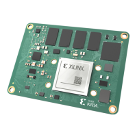
This chapter describes the electrical interface details needed to design your carrier card to mate
with the Kria™ K26 SOM. The electrical interface design guidelines include the SOM connector
details and signal names, signal roung guidelines, and power supply design.
SOM Connector Overview
The K26 SOM uses two 240-pin connectors to provide electrical connecvity between the SOM
and the carrier card. These two connectors are referred to as SOM240_1 and SOM240_2.
The SOM240_1 and SOM240_2 connectors use the Samtec 0.635 mm AcceleRate HD high-
density 4-row, 60 posion connector set. The part number for the socket (ADF6–60–03.5–L–4–
2–A) is used on the boom side of the SOM. The part number for the terminal (ADM6–60–
01.5–L–4–2–A) is for use on the carrier card. The SOM240_1 and SOM240_2 connectors
provide support for following interfaces.
• Control and status signals
• Mulplexed I/O (MIO) bank
• PS-GTR high-speed serial transceiver signals
• High-performance I/O (HPIO) bank signals
• High-density I/O (HDIO) bank signals
• GTH high-speed serial transceiver signals
• Power system
Signal Naming Conventions
The SOM240 connectors adopt the naming convenons outlined in the following table.
Chapter 2: Electrical Design Considerations
UG1091 (v1.0) April 20, 2021 www.xilinx.com
Carrier Card Design for Kria SOM 7
 Loading...