DSP-AX1/RX-V1
DSP-AX1/RX-V1
42
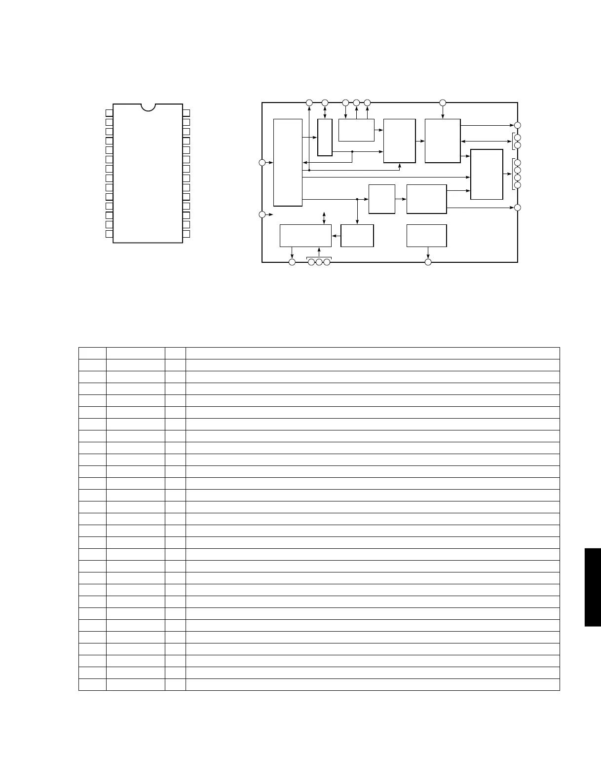
IC2 : YSD917 (P.C.B. DSP)
DIR5 (Digital Format Interface Receiver)
No. Name I/O Function
1 AVDD Analog power supply for PLL (+5V)
2 PCO A PLL filter connecting terminal
3 AVSS Analog ground
4 M/S Is+ Master/slave mode selection
5 DDIN Is Digital audio interface data input
6 TEST Is+ Test terminal (to be open)
7 /IC Is Initial clear input
8 VSS Ground
9 XO O 24.576MHz crystal oscillator connecting terminal (output)
10 XI I 24.576MHz crystal oscillator connecting terminal (input)
11 MCK O 12.288MHz clock output terminal
12 VDD +5V power supply
13 SDO O Serial data output
14 SDBCK Is/O Serial data bit clock input/output 64fs
15 SDWCK I/O Serial data word clock input/output fs
16 SDMCK O Serial data master clock output 256fs or 128fs
17 VSS Ground
18 SYNC/U O Serial data synchronous timing output / user data output
19 FS128/C O Serial data master clock 128fs output / channel status output
20 DBL/V O Double rate clock output / validity flag output
21 ERR/BS O Data error detect output / block start output
22 /LOCK O PLL lock detect output
23 INT O Interrupt output
24 VDD +5V power supply
25 /CS I Microprocessor interface chip select input
26 SO Ot Microprocessor interface data output
27 SI I Microprocessor interface data input
28 SCK Is Microprocessor interface bit clock input
Is: Schmidt trigger input terminal
I+: Input terminal with pull-up resistor
O: digital output terminal
Ot: Tri-state digital output terminal
A: Analog terminal
With SYNC/U, FS128, DBL/V and ERR/BS, select each function by setting the control register.
1
2
3
4
5
6
7
8
9
10
11
12
13
14
28
27
26
25
24
23
22
21
20
19
18
17
16
15
AVDD
PCO
AVSS
M/S
DDIN
TEST
/IC
VSS
XO
XI
MCK
VDD
SDO
SDBCK
SCK
SI
SO
/CS
VDD
INT
/LOCK
ERR/BS
DBL/V
FS128/C
SYNC/U
VSS
SDMCK
SDWCK
DIGITAL AUDIO INTERFACE
DECODER &
LOCK ERROR JUDGMENT
PLL
STANDARD
CLOCK
GENERATION
CLOCK
SYSTEM
SELECTION
OUTPUT
CLOCK
GENERATION
OUTPUT
SELECTION
MICROPROCESSOR
INTERFACE
EACH CONTROL
SIGNAL
DATA BUS
CHANNEL
STATUS
USER DATA
FRAME
BUFFER
SERIAL
CONVERSION
INTERRUPT
FACTOR
DETECTION
5
7
26
22 2 10 9 11 4
28 23
13
18
19
20
21
14
15
16
2725
DDIN
/IC
SO
/CS
SI
SCK
INT
SDO
ERR/BS
DBL/V
FS128/C
SYNC/U
SDBCK
SDWCK
SDMCK
/LOCK
PCO
XI
XO
MCK
M/S
 Loading...