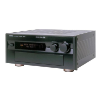
DSP-AX1/RX-V1
DSP-AX1/RX-V1
44
IC5 : YSS908 (P.C.B. DSP)
AC3Dav
No. Name I/O Function
1 PVDD +5V power supply
2 RAMCEN O External SRAM chip enable terminal
3 RAMA16 O External SRAM address terminal 16
4 RAMA15 O External SRAM address terminal 15
5 SDIB0 I PCM input terminal 0 to Sub DSP
6 SDIB1 I PCM input terminal 1 to Sub DSP
7 SDIB2 I PCM input terminal 2 to Sub DSP
8 XI I Crystal oscillator connecting terminal (12.288MHz )
9 XO O Crystal oscillator connecting terminal
10 PVSS Ground terminal (for digital)
11 AVDD +3V power terminal (for analog)
12 TEST Test terminal (unconnected)
13 TEST Test terminal (unconnected)
14 TEST Test terminal (unconnected)
15 OVFB O Sub DSP overflow detect terminal
16 TEST Test terminal (unconnected)
17 TEST Test terminal (unconnected)
18 TEST Test terminal (unconnected)
19 CPO O PLL output terminal (connected to external analog filter circuit)
20 AVSS Ground terminal (for PLL circuit)
21 VDD2 +3.3V power terminal (for internal circuit)
22 SDOA2 O PCM output terminal from Main DSP (C/LFE output at AC-3/DTS, C/S output at Pro Logic)
23 SDOA1 O PCM output terminal from Main DSP (LS/RS output at AC-3/DTS, Lt/Rt output at Pro Logic)
24 SDOA0 O PCM output terminal from Main DSP (L/R output at both AC-3/DTS and Pro Logic)
25 RAMA14 O External SRAM address terminal 14
26 RAMA13 O External SRAM address terminal 13
27 RAMA12 O External SRAM address terminal 12
28 RAMA11 O External SRAM address terminal 11
29 RAMA10 O External SRAM address terminal 10
30 VSS Ground terminal (for internal circuit)
31 PVDD +5V power terminal
32 OPORT0 O General purpose output terminal (L/R ch is shifted by +3dB at Dolby Pro Logic)
33 OPORT1 O General purpose output terminal (N.C.)
34 OPORT2 O General purpose output terminal (N.C.)
35 OPORT3 O General purpose output terminal (N.C.)
36 OPORT4 O General purpose output terminal (N.C.)
37 OPORT5 O General purpose output terminal (N.C.)
38 OPORT6 O General purpose output terminal (N.C.)
39 OPORT7 O General purpose output terminal (N.C.)
40 VSS Ground terminal (for internal circuit)
41 VDD +3V power terminal
42 RAMA9 O External SRAM address terminal 9
43 RAMA8 O External SRAM address terminal 8
44 RAMA7 O External SRAM address terminal 7
45 SDOB2 O PCM output terminal from Sub DSP
46 SDOB1 O PCM output terminal from Sub DSP
47 SDOB0 O PCM output terminal from Sub DSP
48 SDBCK1 I Bit clock input terminal for SDOA, SDIB, SDOB signals
49 SDWCK1 I Word clock input terminal for SDOA, SDIB, SDOB signals
50 VSS Ground terminal
51 VDD +3V power terminal
52 AC3DATA O AC-3 data output terminal, AC-3 bit stream data detect
 Loading...