Page
3.8
General Theory of Operation
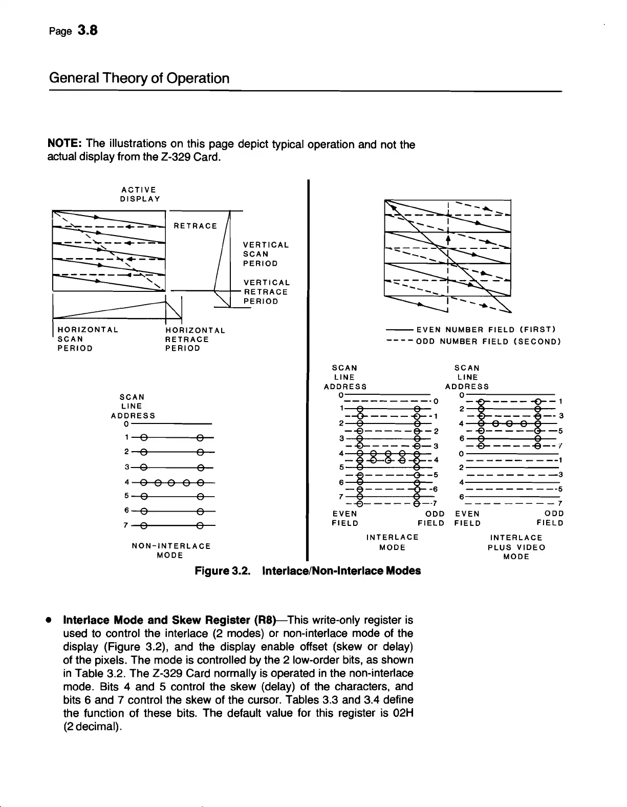
NOTE: The illustrations on this page depict typical operation
and
not the
actual display from the Z-329 Card.
--
EVEN
NUMBER
FIELD
(FIRST)
--
- -
ODD
NUMBER
FIELD
(SECOND)
VERTICAL
SCAN
PERIOD
VERTICAL
L-
.:::=::::::.0..1
------+--+-
RE
TRAC
E
I
~
PERIOD
~HORIZONTAL
SCAN
RETRACE
PERIOD
PERIOD
ACTIVE
DISPLAY
NON-INTERLACE
MODE
SCAN
LINE
ADDRESS
o
_~
-()--1
:-S-oo-ot-- 3
-
-e-
- - - -8:
-5
6 0 0
--e-----~--l
0-------
----------1
2-------
---
---
---3
4-------
---------·5
6-------
---------7
EVEN
ODD
FIELD
FIELD
INTERLACE
PLUS
VIDEO
MODE
SCAN
LINE
ADDRESS
0-------
---------·0
1
~
0
2
--g-
--
--
Z--1
--e-----o--2
3
<Y
0
-~----_e-3
:-8z:g:~t--4
6
-!-----<r-
5
7
-~----=f-6
--e-----e--7
EVEN
ODD
FIELD FIELD
INTERLACE
MODE
o
o
o
o
o
o
o
0
4
000
2 0
3 0
5 0
6 0
7 0
SCAN
LINE
ADDRESS
0------
1 0
Figure 3.2. Interlace/Non-Interlace Modes
• Interlace Mode and Skew Register
(R8)-
This write-only register is
used
to
control the interlace
(2
modes) or non-interlace mode of the
display (Figure 3.2), and the display enable offset (skew or delay)
of the pixels. The mode is controlled
by
the 2 low-order bits, as shown
in
Table 3.2. The Z-329 Card normally
is
operated
in
the non-interlace
mode. Bits 4 and 5 control the skew (delay) of the characters,
and
bits 6 and 7 control the skew of the cursor. Tables 3.3
and
3.4 define
the function of these bits. The default value for this register is
02H
(2
decimal).



 To Next Page